


© Koninklijke Philips Electronics N.V. 2005. All rights reserved.
User manual Rev. 02 — 23 May 2005 71 of 133
Philips Semiconductors
UM10109
P89LPC932A1 User manual
11.3 I
2
C control register
The CPU can read and write this register. There are two bits are affected by hardware: the
SI bit and the STO bit. The SI bit is set by hardware and the STO bit is cleared by
hardware.
CRSEL determines the SCL source when the I
2
C-bus is in master mode. In slave mode
this bit is ignored and the bus will automatically synchronize with any clock frequency up
to 400 kHz from the master I
2
C device. When CRSEL = 1, the I
2
C interface uses the
Timer 1 overflow rate divided by 2 for the I
2
C clock rate. Timer 1 should be programmed
by the user in 8 bit auto-reload mode (Mode 2).
Data rate of I
2
C-bus = Timer overflow rate / 2 = PCLK / (2*(256-reload value)).
If f
osc
= 12 MHz, reload value is 0 to 255, so I
2
C data rate range is 11.72 Kbit/sec to
3000 Kbit/sec.
When CRSEL = 0, the I
2
C interface uses the internal clock generator based on the value
of I2SCLL and I2CSCLH register. The duty cycle does not need to be 50 %.
The STA bit is START flag. Setting this bit causes the I
2
C interface to enter master mode
and attempt transmitting a START condition or transmitting a repeated START condition
when it is already in master mode.
The STO bit is STOP flag. Setting this bit causes the I
2
C interface to transmit a STOP
condition in master mode, or recovering from an error condition in slave mode.
If the STA and STO are both set, then a STOP condition is transmitted to the I
2
C-bus if it is
in master mode, and transmits a START condition afterwards. If it is in slave mode, an
internal STOP condition will be generated, but it is not transmitted to the bus.
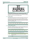
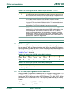
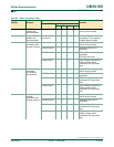
Table 61: I
2
C Control register (I2CON - address D8h) bit allocation
Bit 7 6 5 4 3 2 1 0
Symbol - I2EN STA STO SI AA - CRSEL
Resetx00000x0
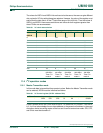
Table 62: I
2
C Control register (I2CON - address D8h) bit description
Bit Symbol Description
0 CRSEL SCL clock selection. When set = 1, Timer 1 overflow generates SCL, when cleared
= 0, the internal SCL generator is used base on values of I2SCLH and I2SCLL.
1- reserved
2 AA The Assert Acknowledge Flag. When set to 1, an acknowledge (low level to SDA)
will be returned during the acknowledge clock pulse on the SCL line on the
following situations:
(1)The ‘own slave address’ has been received. (2)The general call address has
been received while the general call bit (GC) in I2ADR is set. (3) A data byte has
been received while the I
2
C interface is in the Master Receiver Mode. (4)A data
byte has been received while the I
2
C interface is in the addressed Slave Receiver
Mode. When cleared to 0, an not acknowledge (high level to SDA) will be returned
during the acknowledge clock pulse on the SCL line on the following situations: (1)
A data byte has been received while the I
2
C interface is in the Master Receiver
Mode. (2) A data byte has been received while the I
2
C interface is in the addressed
Slave Receiver Mode.