


© Koninklijke Philips Electronics N.V. 2005. All rights reserved.
User manual Rev. 02 — 23 May 2005 38 of 133
Philips Semiconductors
UM10109
P89LPC932A1 User manual
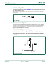
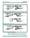
6.1 Reset vector
Following reset, the P89LPC932A1 will fetch instructions from either address 0000h or the
Boot address. The Boot address is formed by using the Boot Vector as the high byte of the
address and the low byte of the address = 00h. The Boot address will be used if a UART
break reset occurs or the non-volatile Boot Status bit (BOOTSTAT.0) = 1, or the device has
been forced into ISP mode. Otherwise, instructions will be fetched from address 0000H.
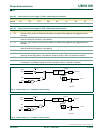
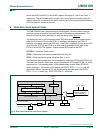
7. Timers 0 and 1
The P89LPC932A1 has two general-purpose counter/timers which are upward compatible
with the 80C51 Timer 0 and Timer 1. Both can be configured to operate either as timers or
event counters (see Tabl e 20
). An option to automatically toggle the Tx pin upon timer
overflow has been added.
In the ‘Timer’ function, the timer is incremented every PCLK.
In the ‘Counter’ function, the register is incremented in response to a 1-to-0 transition on
its corresponding external input pin (T0 or T1). The external input is sampled once during
every machine cycle. When the pin is high during one cycle and low in the next cycle, the
count is incremented. The new count value appears in the register during the cycle
following the one in which the transition was detected. Since it takes two machine cycles
(four CPU clocks) to recognize a 1-to-0 transition, the maximum count rate is
1
⁄
4
of the
CPU clock frequency. There are no restrictions on the duty cycle of the external input
signal, but to ensure that a given level is sampled at least once before it changes, it should
be held for at least one full machine cycle.
The ‘Timer’ or ‘Counter’ function is selected by control bits TnC/T
(x = 0 and 1 for Timers 0
and 1 respectively) in the Special Function Register TMOD. Timer 0 and Timer 1 have five
operating modes (modes 0, 1, 2, 3 and 6), which are selected by bit-pairs (TnM1, TnM0)
in TMOD and TnM2 in TAMOD. Modes 0, 1, 2 and 6 are the same for both
Timers/Counters. Mode 3 is different. The operating modes are described later in this
section.
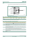
Table 19: Timer/Counter Mode register (TMOD - address 89h) bit allocation
Bit 7 6 5 4 3 2 1 0
Symbol T1GATE T1C/T
T1M1 T1M0 T0GATE T0C/T T0M1 T0M0
Reset00000000
Table 20: Timer/Counter Mode register (TMOD - address 89h) bit description
Bit Symbol Description
0 T0M0 Mode Select for Timer 0. These bits are used with the T0M2 bit in the TAMOD register to determine the
Timer 0 mode (see Ta bl e 22
).
1T0M1
2T0C/T
Timer or Counter selector for Timer 0. Cleared for Timer operation (input from CCLK). Set for Counter
operation (input from T0 input pin).
3 T0GATE Gating control for Timer 0. When set, Timer/Counter is enabled only while the INT0
pin is high and the TR0
control pin is set. When cleared, Timer 0 is enabled when the TR0 control bit is set.