


© Koninklijke Philips Electronics N.V. 2005. All rights reserved.
User manual Rev. 02 — 23 May 2005 36 of 133
Philips Semiconductors
UM10109
P89LPC932A1 User manual
6. Reset
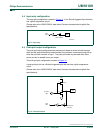
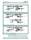
The P1.5/RST pin can function as either an active low reset input or as a digital input,
P1.5. The RPE (Reset Pin Enable) bit in UCFG1, when set to 1, enables the external reset
input function on P1.5. When cleared, P1.5 may be used as an input pin. When using an
oscillator frequency above 12 MHz, the reset input function of P1.5 must be
enabled. An external circuit is required to hold the device in reset at powerup until
V
DD
has reached its specified level. When system power is removed V
DD
will fall
below the minimum specified operating voltage. When using an oscillator
frequency above 12 MHz, in some applications, an external brownout detect circuit
may be required to hold the device in reset when V
DD
falls below the minimum
specified operating voltage.
Note: During a power-on sequence, The RPE selection is overridden and this pin will
always functions as a reset input. An external circuit connected to this pin should not hold
this pin low during a Power-on sequence as this will keep the device in reset. After
power-on this input will function either as an external reset input or as a digital input as
defined by the RPE bit. Only a power-on reset will temporarily override the selection
defined by RPE bit. Other sources of reset will not override the RPE bit.
Note: During a power cycle, V
DD
must fall below V
POR
(see P89LPC932A1 data sheet,
Static characteristics) before power is reapplied, in order to ensure a power-on reset.
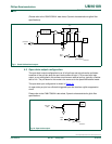
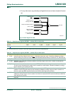
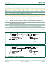
Reset can be triggered from the following sources (see Figure 13
):
• External reset pin (during power-on or if user configured via UCFG1);
• Power-on Detect;
• Brownout Detect;
• Watchdog Timer;
• Software reset;
• UART break detect reset.
For every reset source, there is a flag in the Reset Register, RSTSRC. The user can read
this register to determine the most recent reset source. These flag bits can be cleared in
software by writing a logic 0 to the corresponding bit. More than one flag bit may be set:
• During a power-on reset, both POF and BOF are set but the other flag bits are
cleared.
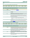
4- reserved
5 VCPD Analog Voltage Comparators power-down: When logic 1, the voltage comparators
are powered down. User must disable the voltage comparators prior to setting this
bit.
6 DEEPD Data EEPROM power-down: When logic 1, the Data EEPROM is powered down.
Note that in either Power-down mode or Total Power-down mode, the Data
EEPROM will be powered down regardless of this bit.
7 RTCPD Real-time Clock power-down: When logic 1, the internal clock to the Real-time
Clock is disabled.
Table 16: Power Control register A (PCONA - address B5h) bit description
…continued
Bit Symbol Description