


© Koninklijke Philips Electronics N.V. 2005. All rights reserved.
User manual Rev. 02 — 23 May 2005 86 of 133
Philips Semiconductors
UM10109
P89LPC932A1 User manual
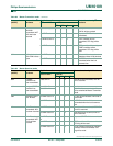
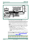
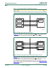
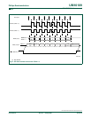
In Figure 38, SSIG (SPCTL.7) for the slave is logic 0, and SS is used to select the slave.
The SPI master can use any port pin (including P2.4/SS
) to drive the SS pin.
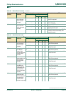
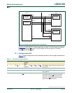
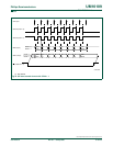
Figure 39
shows a case where two devices are connected to each other and either device
can be a master or a slave. When no SPI operation is occurring, both can be configured
as masters (MSTR = 1) with SSIG cleared to 0 and P2.4 (SS
) configured in
quasi-bidirectional mode. When a device initiates a transfer, it can configure P2.4 as an
output and drive it low, forcing a mode change in the other device (see Section 12.4 “
Mode
change on SS”) to slave.
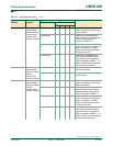
Table 76: SPI Data register (SPDAT - address E3h) bit allocation
Bit 7 6 5 4 3 2 1 0
Symbol MSB LSB
Reset00000000
Fig 38. SPI single master single slave configuration.
Fig 39. SPI dual device configuration, where either can be a master or a slave.
002aaa901
master slave
8-BIT SHIFT
REGISTER
SPI CLOCK
GENERATOR
8-BIT SHIFT
REGISTER
MISO
MOSI
SPICLK
PORT
MISO
MOSI
SPICLK
SS
002aaa90
2
master slave
8-BIT SHIFT
REGISTER
SPI CLOCK
GENERATOR
SPI CLOCK
GENERATOR
8-BIT SHIFT
REGISTER
MISO
MOSI
SPICLK
MISO
MOSI
SPICLK
SS
SS