


© Koninklijke Philips Electronics N.V. 2005. All rights reserved.
User manual Rev. 02 — 23 May 2005 55 of 133
Philips Semiconductors
UM10109
P89LPC932A1 User manual
Setting the PLLEN bit in TCR20 starts the PLL. When PLLEN is set, it will not read back a
one until the PLL is in lock. At this time, the PWM unit is ready to operate and the timer
can be enabled. The following start-up sequence is recommended:
1. Set up the PWM module without starting the timer.
2. Calculate the right division factor so that the PLL receives an input clock signal of
500 kHz - 1 MHz. Write this value to PLLDV.
3. Set PLLEN. Wait until the bit reads one
4. Start the timer by writing a value to bits TMOD21, TMOD20
When the timer runs from the PLL, the timer operates asynchronously to the rest of the
microcontroller. Some restrictions apply:
• The user is discouraged from writing or reading the timer in asynchronous mode. The
results may be unpredictable
• Interrupts and flags are asynchronous. There will be delay as the event may not
actually be recognized until some CCLK cycles later (for interrupts and reads)
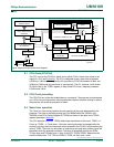
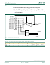
9.11 CCU interrupt structure
There are seven independent sources of interrupts in the CCU: timer overflow, captured
input events on Input Capture blocks A/B, and compare match events on Output Compare
blocks A through D. One common interrupt vector is used for the CCU service routine and
interrupts can occur simultaneously in system usage. To resolve this situation, a priority
encode function of the seven interrupt bits in TIFR2 SFR is implemented (after each bit is
AND-ed with the corresponding interrupt enable bit in the TICR2 register). The order of
priority is fixed as follows, from highest to lowest:
• TOIF2
• TICF2A
• TICF2B
• TOCF2A
• TOCF2B
• TOCF2C
• TOCF2D
An interrupt service routine for the CCU can be as follows:
1. Read the priority-encoded value from the TISE2 register to determine the interrupt
source to be handled.
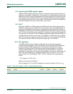
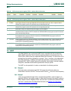
Table 39: CCU control register 1 (TCR21 - address F9h) bit description
Bit Symbol Description
0:3 PLLDV.3:0 PLL frequency divider.
4:6 - Reserved.
7 TCOU2 In basic timer mode, writing a logic 1 to TCOU2 will cause the values to be latched immediately and the
value of TCOU2 will always read as logic 0. In PWM mode, writing a logic 1 to TCOU2 will cause the
contents of the shadow registers to be updated on the next CCU Timer overflow. As long as the latch is
pending, TCOU2 will read as logic 1 and will return to logic 0 when the latching takes place. TCOU2 also
controls the latching of the Output Compare registers OCRAx, OCRBx and OCRCx.