© Koninklijke Philips Electronics N.V. 2005. All rights reserved.
User manual Rev. 02 — 23 May 2005 22 of 133
Philips Semiconductors
UM10109
P89LPC932A1 User manual
The frequency of this clock output is
1
⁄
2
that of the CCLK. If the clock output is not needed
in Idle mode, it may be turned off prior to entering Idle, saving additional power. Note: on
reset, the TRIM SFR is initialized with a factory preprogrammed value. Therefore when
setting or clearing the ENCLK bit, the user should retain the contents of other bits of the
TRIM register. This can be done by reading the contents of the TRIM register (into the
ACC for example), modifying bit 6, and writing this result back into the TRIM register.
Alternatively, the ‘ANL direct’ or ‘ORL direct’ instructions can be used to clear or set bit 6
of the TRIM register.
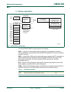
2.4 On-chip RC oscillator option
The P89LPC932A1 has a TRIM register that can be used to tune the frequency of the RC
oscillator. During reset, the TRIM value is initialized to a factory pre-programmed value to
adjust the oscillator frequency to 7.373 MHz, ± 1 %. (Note: the initial value is better than
1 %; please refer to the P89LPC932A1 data sheet for behavior over temperature). End
user applications can write to the TRIM register to adjust the on-chip RC oscillator to other
frequencies. Increasing the TRIM value will decrease the oscillator frequency.
2.5 Watchdog oscillator option
The watchdog has a separate oscillator which has a frequency of 400 kHz. This oscillator
can be used to save power when a high clock frequency is not needed.
2.6 External clock input option
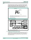
In this configuration, the processor clock is derived from an external source driving the
XTAL1 / P3.1 pin. The rate may be from 0 Hz up to 18 MHz. The XTAL2 / P3.0 pin may be
used as a standard port pin or a clock output. When using an oscillator frequency
above 12 MHz, the reset input function of P1.5 must be enabled. An external circuit
is required to hold the device in reset at powerup until V
DD
has reached its specified
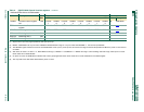
Table 4: On-chip RC oscillator trim register (TRIM - address 96h) bit allocation
Bit 7 6 5 4 3 2 1 0
Symbol RCCLK ENCLK TRIM.5 TRIM.4 TRIM.3 TRIM.2 TRIM.1 TRIM.0
Reset 0 0 Bits 5:0 loaded with factory stored value during reset.
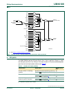
Table 5: On-chip RC oscillator trim register (TRIM - address 96h) bit description
Bit Symbol Description
0 TRIM.0 Trim value. Determines the frequency of the internal RC oscillator. During reset,
these bits are loaded with a stored factory calibration value. When writing to either
bit 6 or bit 7 of this register, care should be taken to preserve the current TRIM value
by reading this register, modifying bits 6 or 7 as required, and writing the result to
this register.
1TRIM.1
2TRIM.2
3TRIM.3
4TRIM.4
5TRIM.5
6 ENCLK when = 1,
CCLK
⁄
2
is output on the XTAL2 pin provided the crystal oscillator is not
being used.
7 RCCLK when = 1, selects the RC Oscillator output as the CPU clock (CCLK). This allows for
fast switching between any clock source and the internal RC oscillator without
needing to go through a reset cycle. The original P89LPC932 required a reset
cycle in order to switch between clock sources.


