C-1
APPENDIX C
REGISTERS
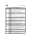
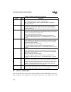
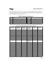
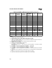
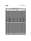
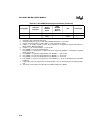
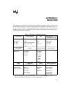
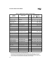
This appendix provides reference information about the device registers. Table C-1 lists the mod-
ules and major components of the device with their related configuration and status registers. Ta-
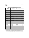
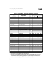
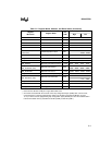
ble C-2 lists the registers, arranged alphabetically by mnemonic, along with their names,
addresses, and reset values. Following the tables, individual descriptions of the registers are ar-
ranged alphabetically by mnemonic.
Table C-1. Modules and Related Registers
A/D Converter Chip Configuration CPU
EPA
(8XC196MC, MH,
x
= 0–3)
(8XC196MD,
x
= 0–5)
AD_COMMAND CCR0 ONES_REG COMP
x
_CON
AD_RESULT CCR1 PSW COMP
x
_TIME
AD_TEST GEN_CON (8XC196MH) SP EPA
x
_CON
AD_TIME PPW (or SP_PPW) ZERO_REG EPA
x
_TIME
USFR
Frequency Generator
(8XC196MD)
I/O Ports Interrupts and PTS Memory Control
FREQ_CNT P
x
_DIR
†
INT_MASK WSR
FREQ_GEN P
x
_MODE
†
INT_MASK1
P
x
_PIN
††
INT_PEND
P
x
_REG
†
INT_PEND1
PI_MASK
PI_PEND
PTSSEL
PTSSRV
PWM
(
x
= 0–1)
Serial Port
(8XC196MH,
x
= 0–1)
Timers
(
x
= 0–1)
Waveform Generator
(
x
= 1–3)
PWM_COUNT SBUF
x
_RX T
x
CONTROL WG_COMP
x
PWM_PERIOD SBUF
x
_TX T1RELOAD WG_CONTROL
PWM
x
_CONTROL SP
x
_BAUD TIMER
x
WG_COUNTER
SP
x
_CON WATCHDOG WG_OUTPUT
SP
x
_STATUS WG_PROTECT
WG_RELOAD
†
For the 8XC196MC,
x
= 2, 5; for the 8XC196MD,
x
= 2, 5, 7; for the 8XC196MH,
x
= 1, 2, 5.
††
For the 8XC196MC and 8XC196MH,
x
= 0–5; for the 8XC196MD,
x
= 0–5, 7.


