6-15
I/O PORTS
6.4.1 Bidirectional Ports 3 and 4 (Address/Data Bus) Operation
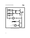
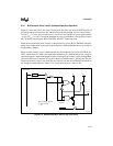
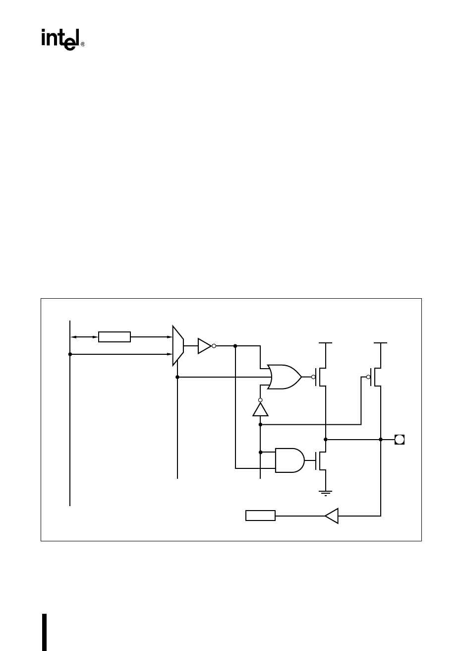
Figure 6-3 shows the ports 3 and 4 logic. During reset, the active-low level of RESET# turns off
Q1 and Q2 and turns on transistor Q3, which weakly pulls the pin high. (Q1 can source at least –
3 mA at V
CC
–0.7 volts; Q2 can sink at least 3 mA at 0.45 volts; and Q3 can source approximately
–10 µΑ at V
CC
–1.0 volts. Consult the datasheet for exact specifications.) During normal opera-
tion, an internal control signal, BUS CONTROL SELECT, controls the port.
When the microcontroller needs to access external memory, it clears BUS CONTROL SELECT,
which selects address/data as the input to the multiplexer. Address/data then drives Q1 and Q2 as
complementary outputs.
When external memory access is not required, the microcontroller sets BUS CONTROL SE-
LECT, which selects Px_REG as the input to the multiplexer. Px_REG then drives Q1 and Q2 as
open-drain outputs. (Open-drain outputs require external pull-up resistors.) In this configuration,
a port pin can be used as an input. The signal on the pin is latched in the Px_PIN register. The pins
can be read, making it easy to see which pins are driven low by the microcontroller and which are
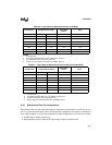
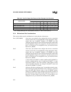
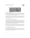
driven high by external drivers. Table 6-13 is a logic table for ports 3 and 4 as I/O.
Figure 6-3. Address/Data Bus (Ports 3 and 4) Structure
Internal Bus
Address/Data
A3116-01
V
CC
V
CC
I/O Pin
RESET#
1
0
BUS CONTROL SELECT
0 = Address/Data
1 = I/O
Px_PIN
Q1 Q3
Q2
Px_REG


