13-5
MINIMUM HARDWARE CONSIDERATIONS
If the A/D converter will be used, connect V
REF
to a separate reference supply to minimize noise
during A/D conversions. Even if the A/D converter will not be used, V
REF
and ANGND must be
connected to provide power to port 0. On the 8XC196MC and MD, they also provide power to
port 1. Refer to “Analog Ground and Reference Voltages” on page 12-12 for a detailed discussion
of A/D power and ground recommendations.
Multilayer printed circuit boards with separate V
CC
and ground planes also help to minimize
noise. For more information on noise protection, refer to AP-125, Designing Microcontroller Sys-
tems for Noisy Environments and AP-711, EMI Design Techniques for Microcontrollers in Auto-
motive Applications.
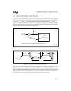
13.4 THE ON-CHIP OSCILLATOR CIRCUITRY
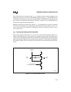
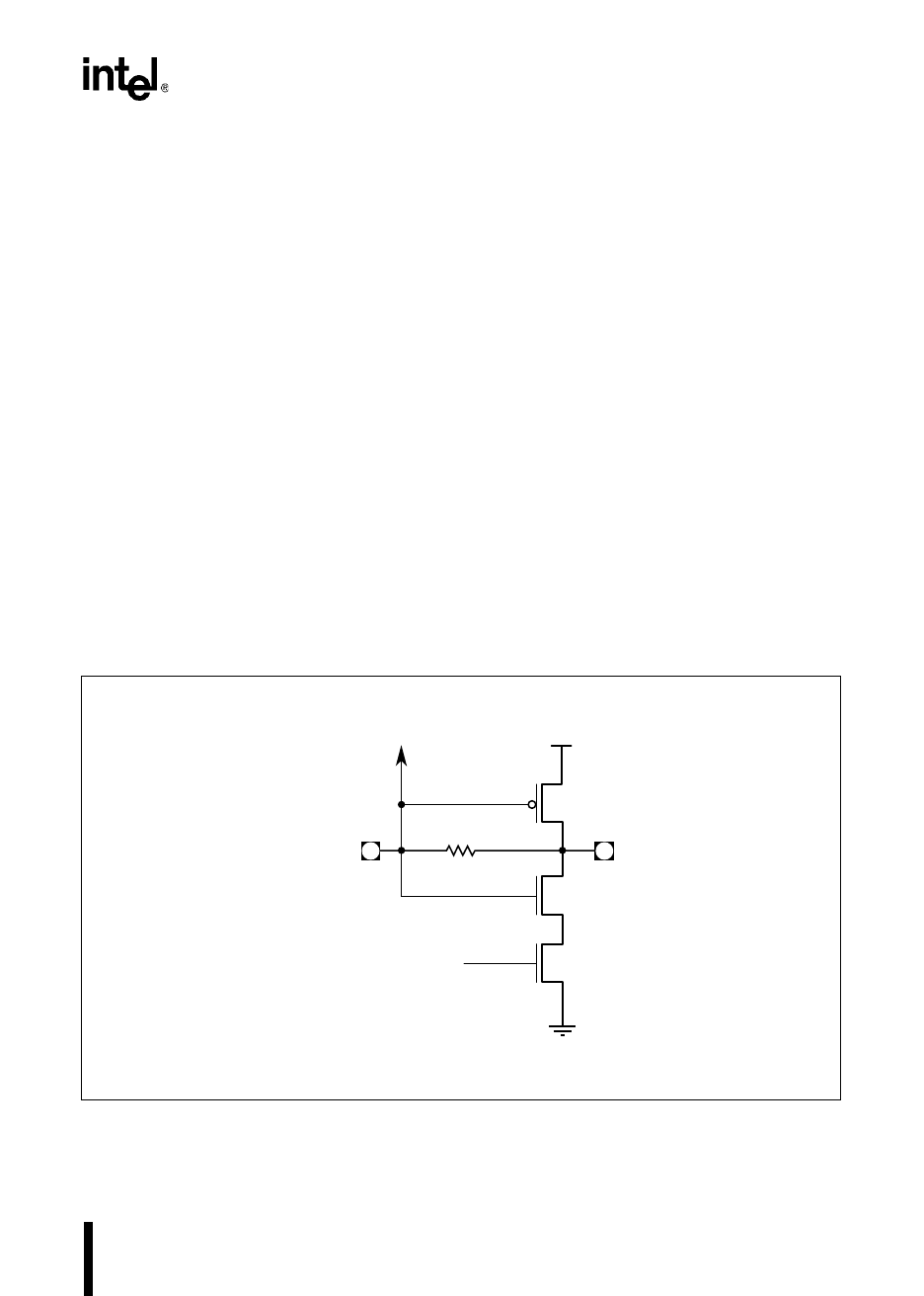
The on-chip oscillator circuit (Figure 13-3) consists of a crystal-controlled, positive reactance os-
cillator. In this application, the crystal operates in a parallel resonance mode. The feedback resis-
tor, Rf, consists of paralleled n-channel and p-channel FETs controlled by the internal powerdown
signal. In powerdown mode, Rf acts as an open and the output drivers are disabled, which disables
the oscillator. Both the XTAL1 and XTAL2 pins have built-in electrostatic discharge (ESD) pro-
tection.
Figure 13-3. On-chip Oscillator Circuit
Rf
XTAL2
(Output)
V
CC
XTAL1
(Input)
Oscillator Enable#
(from powerdown circuitry)
To internal
circuitry
A0076-03
V
SS


