8XC196MC, MD, MH USER’S MANUAL
12-10
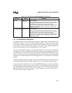
12.6 DESIGN CONSIDERATIONS
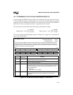
This section describes considerations for the external interface circuitry and describes the errors
that can occur in any A/D converter. The datasheet lists the absolute error specification, which
includes all deviations between the actual conversion process and an ideal converter. However,
because the various components of error are important in many applications, the datasheet also
lists the specific error components. This section describes those components. For additional in-
formation and design techniques, consult AP-406, MCS
®
96 Analog Acquisition Primer (order
number 270365). Application note AP-406 is also included in the Embedded Microcontrollers
handbook.
12.6.1 Designing External Interface Circuitry
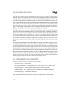
The external interface circuitry to an analog input is highly dependent upon the application and
can affect the converter characteristics. Factors such as input pin leakage, sample capacitor size,
and multiplexer series resistance from the input pin to the sample capacitor must be considered
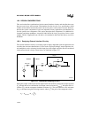
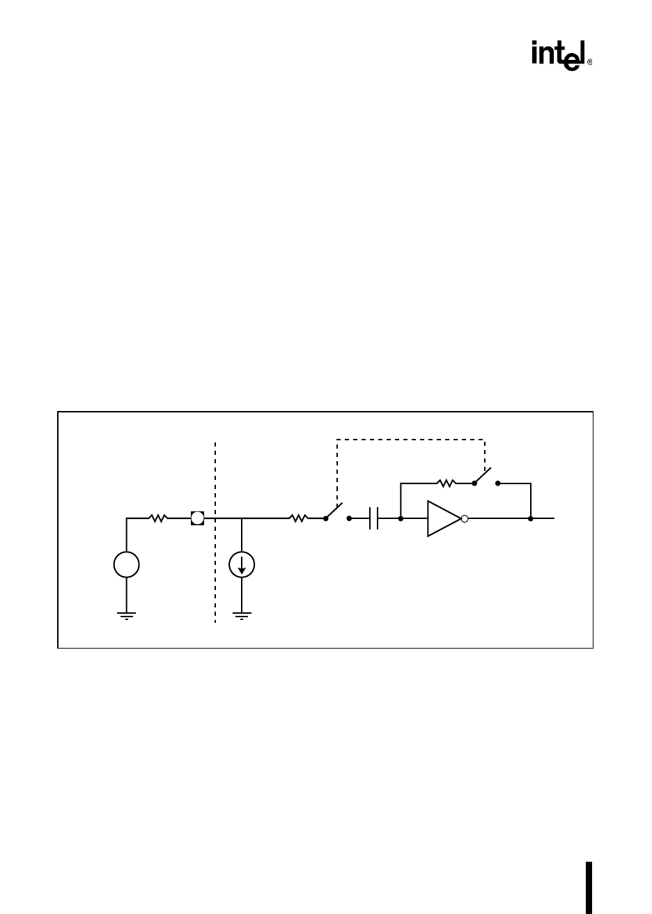
in the external circuit’s design. These factors are idealized in Figure 12-7.
Figure 12-7. Idealized A/D Sampling Circuitry
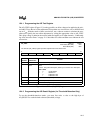
During the sample window, the external input circuit must be able to charge the sample capacitor
(C
S
) through the series combination of the input source resistance (R
SOURCE
), the input series re-
sistance (R
1
), and the comparator feedback resistance (R
F
). The total effective series resistance
(R
T
) is calculated using the following formula, where A
V
is the gain of the comparator circuit.
Leakage
V
R
SOURCE
+
-
C
S
R1
~1KΩ
~2pF
I
LI1
External Internal
A
V
R
F
Sample
A0243-02
R
T
R
SOURCE
R
1
R
F
A
V
1+
----------------
++=


