8XC196MC, MD, MH USER’S MANUAL
10-2
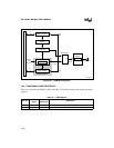
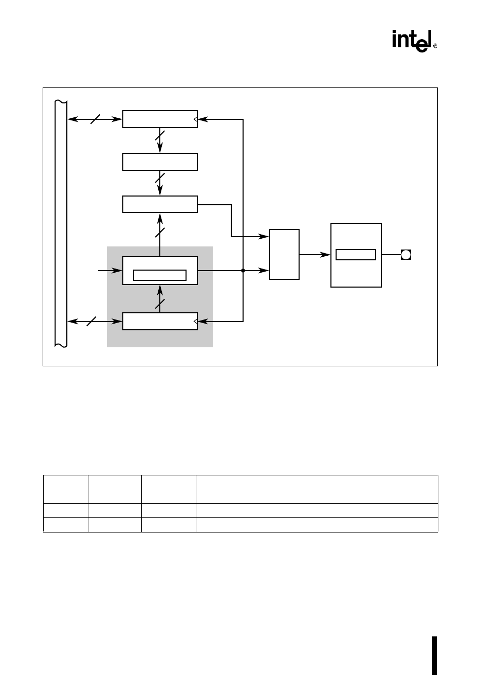
Figure 10-1. PWM Block Diagram
10.2 PWM SIGNALS AND REGISTERS
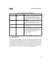
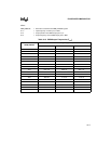
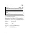
Table 10-1 describes the PWM’s signals and Table 10-2 briefly describes the control and status
registers.
Table 10-1. PWM Signals
Port Pin
PWM
Signal
PWM
Signal Type
Description
P6.6 PWM0 O Pulse-width modulator 0 output with high-drive capability.
P6.7 PWM1 O Pulse-width modulator 1 output with high-drive capability.
A2761-02
PWM
x
_CONTROL
R
S
Q
Port 6
Control
WG_OUT
P6.x/PWM
x
8
8
Buffer
x
8
Comparator
x
8
Down Counter
8
PWM_COUNT
PWM_PERIOD
8
PWM
x
Output
Count
= 00H
Load
=
Load
Buffer
Internal
Clock
Signal
RS Flip-flop
x
Shared Circuitry


