8XC196MC, MD, MH USER’S MANUAL
13-8
13.6 RESETTING THE DEVICE
Reset forces the device into a known state. As soon as RESET# is asserted, the I/O pins, the con-
trol pins, and the registers are driven to their reset states. (Tables in Appendix B list the reset states
of the pins (see Table B-8 on page B-23 for the 8XC196MC and 8XC196MD or Table B-9 on
page B-25 for the 8XC196MH). See Table C-2 on page C-2 for the reset values of the SFRs.) The
device remains in its reset state until RESET# is deasserted. When RESET# is deasserted, the bus
controller fetches the chip configuration bytes (CCBs), loads them into the chip configuration
registers (CCRs), and then fetches the first instruction.
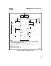
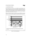
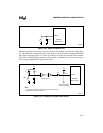
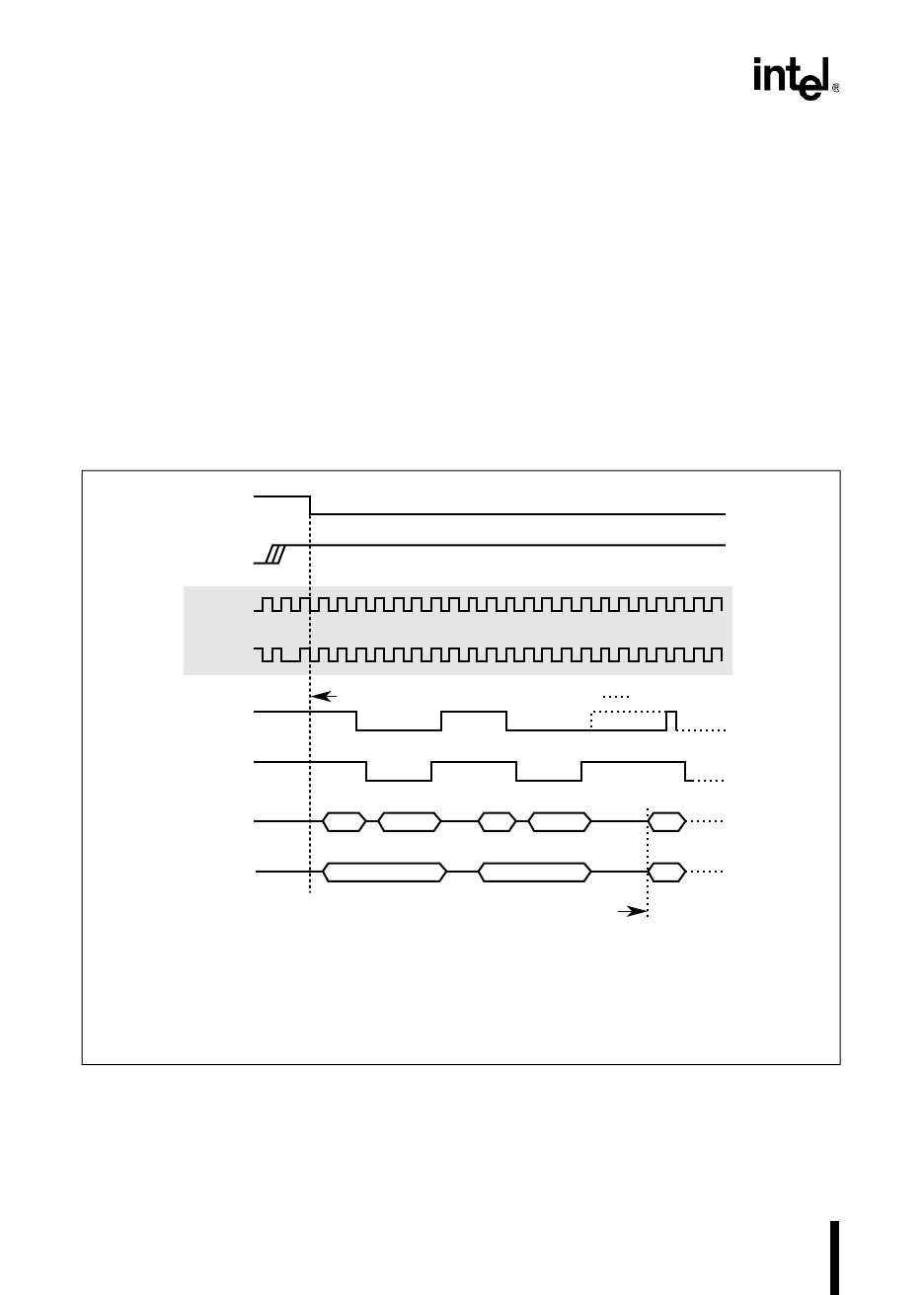
Figure 13-7 shows the reset-sequence timing. Depending upon when RESET# is brought high,
the CLKOUT signal (MC and MD only) may become out of phase with the PH1 internal clock.
When this occurs, the clock generator immediately resynchronizes CLKOUT as shown in Case 2.
Figure 13-7. Reset Timing Sequence
RESET#
Pin
Case 1
CLKOUT
Case 2
CLKOUT
Internal
Reset
ALE
CCB0 CCB1
Phases Resynchronized
RD#
AD7:0
Bus parameters defined by CCB0 (ready
control, bus width, and bus-timing
modes) take effect here.
18H 1AH 80H
20H20H
20H
†
Weak
†
Weak
†Defaults to an 8-bit bus until the CCBs are loaded. AD15:8 weakly drive address during the CCB fetches.
For 16-bit systems, write 20H to the high byte of CCB0 and CCB1 (2019H and 201BH) in order to prevent
bus contention.
AD15:8
7 T
XTAL1
7 T
XTAL1
9 T
XTAL1
9 T
XTAL1
= ADV# Selected
9 T
XTAL1
7 T
XTAL1
8 T
XTAL1
11 T
XTAL1
A3088-02
(MC, MD
Only)


