8XC196MC, MD, MH USER’S MANUAL
13-2
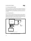
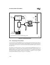
13.1.1 Unused Inputs
For predictable performance, it is important to tie unused inputs to V
CC
or V
SS
. Otherwise, they
can float to a mid-voltage level and draw excessive current. Unused interrupt inputs may generate
spurious interrupts if left unconnected.
13.1.2 I/O Port Pin Connections
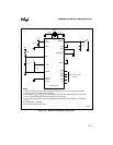
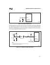
Tie unused input-only port inputs to V
SS
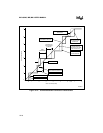
as shown in Figure 13-1. Chapter 6, “I/O Ports,” contains
information about initializing and configuring the ports. Table 13-2 lists the sections, with page
numbers, that contain the information for each port.
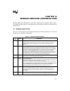
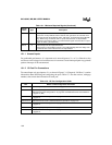
XTAL1 I Input Crystal/Resonator or External Clock Input
Input to the on-chip oscillator and the internal clock generators. The internal clock
generators provide the peripheral clocks, CPU clock, and CLKOUT signal (MC/MD
only). When using an external clock or crystal, instead of the on-chip oscillator,
connect the clock input to XTAL1. The external clock signal must meet the V
IH
speci-
fication for XTAL1 (see datasheet).
XTAL2 O Inverted Output for the Crystal/Resonator
Output of the on-chip oscillator inverter. Leave XTAL2 floating when the design uses
an external clock source instead of the on-chip oscillator.
Table 13-2. I/O Port Configuration Guide
Port Where to Find Configuration Information
Port 0 “Standard Input-only Port Considerations” on page 6-4
Port 1 “Standard Input-only Port Considerations” on page 6-4 (MC, MD)
“Bidirectional Port Pin Configurations” on page 6-9 and “Bidirectional Port Considerations”
on page 6-12 (MH)
Port 2 “Bidirectional Port Pin Configurations” on page 6-9 and “Bidirectional Port Considerations”
on page 6-12
Ports 3 and 4 “Bidirectional Ports 3 and 4 (Address/Data Bus) Operation” on page 6-15
Port 5 “Bidirectional Port Pin Configurations” on page 6-9 and “Bidirectional Port Considerations”
on page 6-12
Port 6 “Configuring Output-only Port Pins” on page 6-17
Port 7 (MD) “Bidirectional Port Pin Configurations” on page 6-9 and “Bidirectional Port Considerations”
on page 6-12
Table 13-1. Minimum Required Signals (Continued)
Signal
Name
Type Description


