15-5
INTERFACING WITH EXTERNAL MEMORY
15.2 CHIP CONFIGURATION REGISTERS AND CHIP CONFIGURATION BYTES
Two chip configuration registers (CCRs) have bits that set parameters for chip operation and ex-
ternal bus cycles. The CCRs cannot be accessed by code. They are loaded from the chip config-
uration bytes (CCBs), which reside in nonvolatile memory at addresses 2018H (CCB0) and
201AH (CCB1).
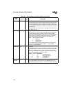
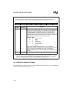
P5_REG 1FF5H Port 5 Data Output
For an input, regardless of the pin’s configuration, set the corresponding
P5_REG bit.
For an output, write the data to be driven out by each pin to the corre-
sponding bit of P5_REG. When a pin is configured as standard I/O
(P5_MODE.
y
= 0), the result of a CPU write to P5_REG is immediately
visible on the pin. When a pin is configured as a special-function signal
(P5_MODE.
y
= 1), the associated on-chip peripheral or off-chip component
controls the pin. The CPU can still write to P5_REG, but the pin is unaffected
until it is switched back to its standard I/O function.
This feature allows software to configure a pin as standard I/O (clear
P5_MODE.
y
), initialize or overwrite the pin value, then configure the pin as a
special-function signal (set P5_MODE.
y
). In this way, initialization, fault
recovery, exception handling, etc., can be done without changing the
operation of the associated peripheral.
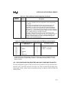
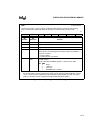
Table 15-3. Register Settings for Configuring External Memory Interface Signals
Port Pin
External Memory Interface
Signal Name
Signal Type Port Register Settings
P5.0
P5.1
P5.2
P5.3
P5.5
P5.6
P5.7
ALE/ADV#
INST
WR#/WRL#
†
RD#
BHE#/WRH#
†
READY
BUSWIDTH (K
x
)
O
O
O
O
O
I
I
P5_DIR = 110X 0000B
P5_MODE = 111X 1111B
P5_REG = 11XX XXXXB
†
The chip configuration register 0 (CCR0), which is loaded at reset from the chip configuration byte 0
(CCB0, 2018H) during normal operation, determines whether P5.2 functions as BHE# or WRH# and
whether P5.5 functions as WR# or WRL#. CCR0.2 = 1 selects BHE# and WR#; CCR0.2 = 1 selects
WRH# and WRL#.
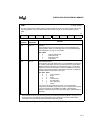
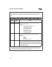
Table 15-2. External Memory Interface Registers (Continued)
Register
Mnemonic
Address Description


