15-27
INTERFACING WITH EXTERNAL MEMORY
15.5.3 Address Valid Strobe Mode
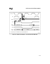
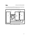
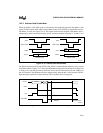
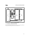
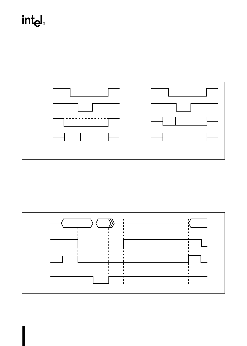
When the address valid strobe mode is selected, the microcontroller generates the address valid
signal (ADV#) instead of the address latch enable signal (ALE). ADV# is asserted after an exter-
nal address is valid (see Figure 15-16). This signal can be used to latch the valid address and si-
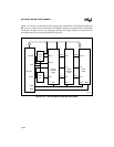
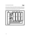
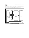
multaneously enable an external memory device. (See the examples in Figures 15-18 and 15-19.)
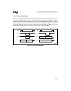
Figure 15-16. Address Valid Strobe Mode
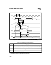
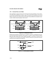
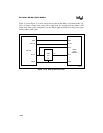
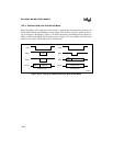
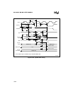
The difference between ALE and ADV# is that ADV# is asserted for the entire bus cycle, not just
to latch the address. Figure 15-17 shows the difference between ALE and ADV# for a single read
or write cycle. Note that for back-to-back bus access, the ADV# function will look identical to
the ALE function. The difference becomes apparent only when the bus is idle. Because ADV# is
high during these periods, external memory will be disabled, thus saving power.
Figure 15-17. Comparison of ALE and ADV# Bus Cycles
ADV#
WR# or RD#
BHE#
AD15:0
Valid
Data OutAddress
16-bit Bus Cycle 8-bit Bus Cycle
Address High
Data Out
ADV#
WR# or RD#
AD7:0
AD15:8
Addr
Low
A3092-02
Address
Data
ADV#
ALE
RD#, WR#
Next Bus Cycle
Bus Idle
A3093-02
AD15:0


