9-17
WAVEFORM GENERATOR
9.4.4 Specifying the Operating Mode and Dead Time and Starting the Counter
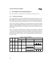
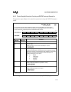
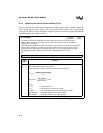
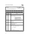
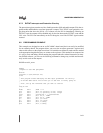
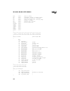
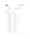
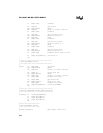
The control register (Figure 9-12) specifies the dead time and operating mode and enables and
disables the counters. A read-only bit (CS) indicates the current count direction.
WG_COMP
x
x
= 1–3
Address:
Reset State:
1FC2H,1FC4H,1FC6H
0000H
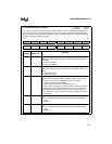
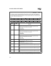
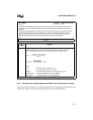
The phase compare (WG_COMP
x
) register controls the duty cycle of each phase. Write a value to
each phase compare register to specify the length of time that the associated outputs will remain
asserted.
Changing the WG_RELOAD value changes both the carrier period and the duty cycle because the
outputs remain asserted for a constant length of time, while the counter takes longer to cycle. To
change the carrier period without changing the duty cycle, you must proportionally change both
WG_RELOAD and WG_COMP
x
at the same time, immediately after the interrupt.
15 0
Compare
Bit
Number
Function
15:0 Compare
These bits determine the length of time that the associated outputs are asserted.
Use the following formulas to calculate output assertion time and duty cycle.
where:
T
OUTPUT
= total time output is asserted, in µs
F
XTAL1
= input frequency on XTAL1 pin, in MHz
multiplier
= 4 for center-aligned modes; 2 for edge-aligned modes
WG_RELOAD = 16-bit WG_RELOAD value ≥ WG_COMP
x
WG_COMP
x
= 16-bit WG_COMP
x
value ≤ WG_RELOAD
Figure 9-11. Phase Compare (WG_COMP
x
) Register
T
OUTPUT
multiplier
WG_COMPx×
F
XTAL1
-----------------------------------------------------------------
=
Duty Cycle
WG_COMPx
WG_RELOAD
--------------------------------------
100%×=


