8XC196MC, MD, MH USER’S MANUAL
15-20
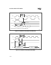
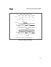
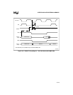
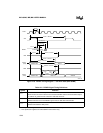
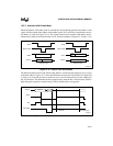
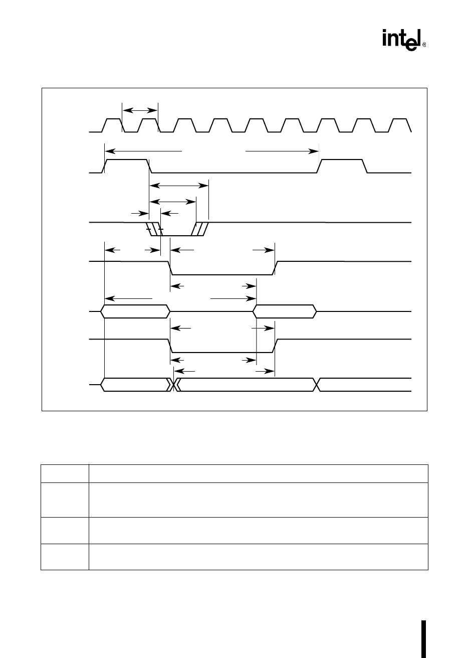
Figure 15-9. READY Timing Diagram — One Wait State (8XC196MH)
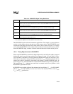
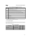
Table 15-5. READY Signal Timing Definitions
Symbol Definition
T
AVYV
Address Valid to READY Setup
Maximum time the external device has to deassert READY after the microcontroller outputs
the address to guarantee that at least one wait state will occur.
T
CLYX
†
READY Hold after CLKOUT Low
Minimum time the level of the READY signal must be valid after CLKOUT falls.
T
LHLH
ALE Cycle Time
Minimum time between ALE pulses.
†
This specification applies to the 8XC196MC, MD microcontrollers only.
††
This specification applies to the 8XC196MH microcontroller only.
XTAL1
A3167-01
T
XTAL1
ALE
T
LHLH
+ 2T
XTAL1
READY
T
LLYV
T
LLYX (min)
T
LLYX (max)
RD#
T
AVYV
T
RLRH
+ 2T
XTAL1
T
RLDV
+ 2T
XTAL1
T
AVDV
+ 2T
XTAL1
Address Out Data In
AD15:0
(read)
WR#
T
QVWH
+ 2T
XTAL1
T
RLDV
+ 2T
XTAL1
T
WLWH
+ 2T
XTAL1
Address Out
AD15:0
(write)
Data Out Address
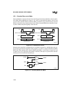
16 MHz 8 MHz


