8XC196MC, MD, MH USER’S MANUAL
6-16
6.4.2 Using Ports 3 and 4 as I/O
To use a port pin as an output, write the output data to the corresponding Px_REG bit. When the
device requires access to external memory, it takes control of the port and drives the address/data
bit onto the pin. The address/data bit replaces your output during this time. When the external ac-
cess is completed, the device restores your data onto the pin.
To use a port pin as an input, set the corresponding Px_REG bit to drive the pin to a high-imped-
ance state. You may then read the pin’s input value in the Px_PIN register. When the device re-
quires access to external memory, it takes control of the port. You must configure the input source
to avoid contention on the bus.
6.4.3 Design Considerations for Ports 3 and 4
When EA# is active, ports 3 and 4 will function only as the address/data bus. In these circum-
stances, an instruction that operates on P3_REG or P4_REG causes a bus cycle that reads from
or writes to the external memory location corresponding to the SFR’s address. (For example, writ-
ing to P4_REG causes a bus cycle that writes to external memory location 1FFDH.) Because
P3_REG and P4_REG have no effect when EA# is active, the bus will float during long periods
of inactivity (such as during a BMOV or TIJMP instruction).
When EA# is inactive, ports 3 and 4 output the contents of the P3_REG and P4_REG registers,
which reset to FFH, placing the pins in a high-impedance state. Ports 3 and 4 will float unless you
either connect external resistors to the pins or write zeros to the P3_REG and P4_REG registers.
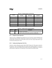
6.5 STANDARD OUTPUT-ONLY PORT 6
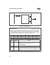
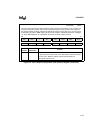
Port 6 is an output-only port that provides output pins for the waveform generator and pulse-width
modulator (PWM). The port 6 pins can be configured to operate either as port pins or as output
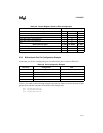
pins for the waveform generator or pulse-width modulator. Table 6-2 lists the pins with their spe-
cial-function signals and associated peripherals.
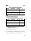
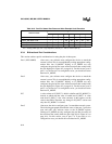
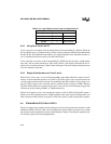
Table 6-13. Logic Table for Ports 3 and 4 as Open-drain I/O
Configuration Open-drain
P
x
_REG 01
Q1 off off
Q2 on off
P
x_
PIN 0 high impedance


