8XC196MC, MD, MH USER’S MANUAL
16-18
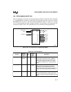
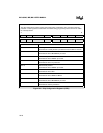
CCR1, CCR0
no direct access
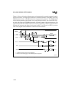
The chip configuration registers (CCRs) control wait states, powerdown mode, and internal memory
protection. These registers are loaded from the PCCBs during programming modes and from the CCBs
for normal operation.
7 0
1 1 0 1 WDE BW1 IRC2 0
7 0
LOC1 LOC0 IRC1 IRC0 ALE WR BW0 PD
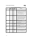
Bit Mnemonic Function
WDE Watchdog Timer Enable
PCCB default is initially disabled (enabled the first time WDT is cleared).
BW1 Buswidth Control
PCCB default selects BUSWIDTH pin control.
IRC2 Internal Ready Control
PCCB default selects READY pin control.
LOC1:0 Security Bits
PCCB default selects no protection.
IRC1:0 Internal Ready Control
PCCB default selects READY pin control.
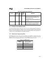
ALE Select Address Valid Strobe Mode
PCCB default selects ALE.
WR Select Write Strobe Mode
PCCB default selects WR# and BHE#.
BW0 Buswidth Control
PCCB default selects BUSWIDTH pin control.
PD Powerdown Enable
PCCB default enables powerdown.
Figure 16-6. Chip Configuration Registers (CCRs)


