


Refresh Control Unit
7-1
CHAPTER
7
REFRESH CONTROL UNIT
7.1 OVERVIEW
The Refresh Control Unit (RCU) automatically generates refresh bus cycles. After a
programmable period of time, the RCU generates a memory read request to the bus
interface unit. The RCU is fixed to three wait states for the PSRAM auto refresh mode.
The Refresh Control Unit operates off the processor internal clock. If the Power-Save mode
is in effect, the Refresh Control Unit must be reprogrammed to reflect the new clock rate.
If the HLDA pin is active when a refresh request is generated (indicating a bus hold
condition), then the microcontroller deactivates the HLDA pin in order to perform a refresh
cycle. The circuit external bus master must remove the HOLD signal for at least one clock
to allow the refresh cycle to execute.
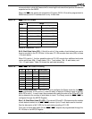
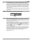
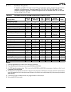
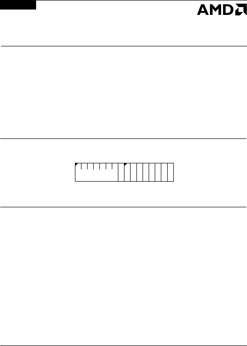
7.1.1 Memory Partition Register (MDRAM, Offset E0h)
Figure 7-1 Memory Partition Register (MDRAM, offset E0h)
The MDRAM Register is set to 0000h on reset.
Bits 15–9: Refresh Base (M6–M0)—Upper bits corresponding to address bits A19–A13
of the 20-bit memory refresh address. Because these bits are available only on the AD bus,
the AD bit must not be set in the LMCS Register if the refresh control unit is used. When
using PSRAM mode, M6–M0 must be programmed to 0000000b.
These bits are cleared to 0 at reset.
Bits 8–0: Reserved—Read back as 0.
15
70
M6–M0
RA19
RA13
000000000