


DMA Controller
10-11
10.4.1 Synchronization Timing
DRQ1 or DRQ0 must be deasserted before the end of the DMA transfer to prevent another
DMA cycle from occurring. The timing for the required deassertion depends on whether
the transfer is source-synchronized or destination-synchronized.
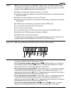
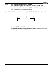
10.4.1.1 Source Synchronization Timing
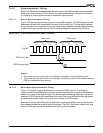
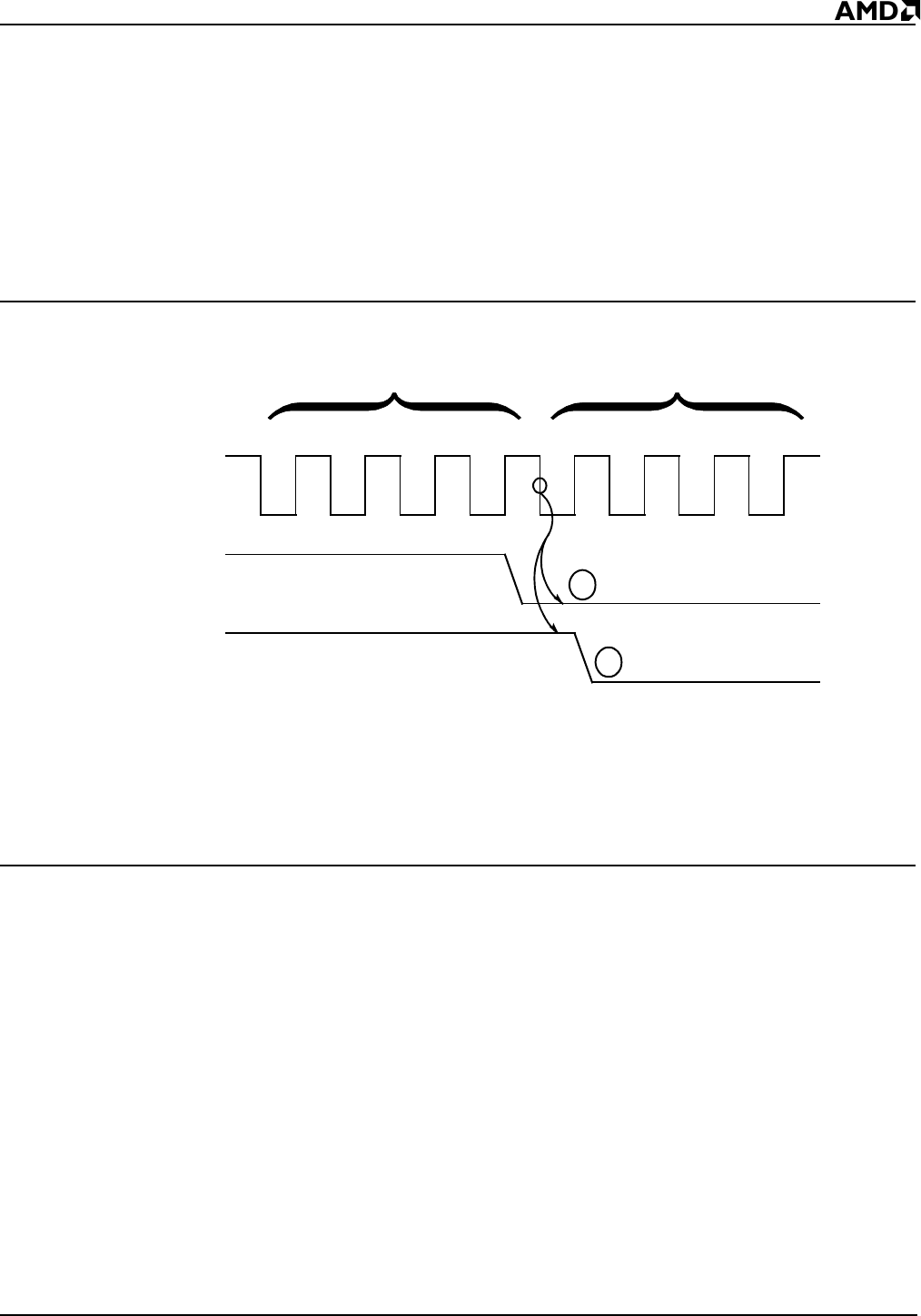
Figure 10-8 shows a typical source-synchronized DMA transfer. The DRQ signal must be
deasserted at least four clocks before the end of the transfer (at T1 of the deposit phase).
If more transfers are not required, a source-synchronized transfer allows the source device
at least three clock cycles from the time it is acknowledged to deassert its DRQ line.
Figure 10-8 Source-Synchronized DMA Transfers
Notes:
1. This source-synchronized transfer is not followed immediately by another DMA transfer.
2. This source-synchronized transfer is immediately followed by another DMA transfer because
DRQ is not deasserted soon enough.
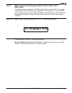
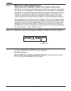
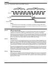
10.4.1.2 Destination Synchronization Timing
Figure 10-9 shows a typical destination-synchronized DMA transfer. A destination-
synchronized transfer differs from a source-synchronized transfer in that two idle states are
added to the end of the deposit cycle. The two idle states allow the destination device to
deassert its DRQ signal four clocks before the end of the cycle. Without the two idle states,
the destination device would not have time to deassert its DRQ signal.
Because of the two extra idle states, a destination-synchronized DMA channel allows other
bus masters to take the bus during the idle states. The CPU, the refresh control unit, and
another DMA channel can all access the bus during the idle states.
T1 T2 T3 T4 T1 T2 T3 T4
CLKOUT
DRQ (First case)
DRQ (Second case)
Fetch Cycle Fetch Cycle
1
2