


Synchronous Serial Interface
12-2
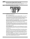
12.1.1 Four-Pin Interface
The SDEN1–SDEN0 pins can be used to enable data transfer individually for as many as
two peripheral devices.
Transmit and receive operations are synchronized between the master (Am186ER or
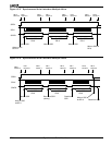
Am188ER microcontroller) and slave (peripheral) by means of the SCLK output. SCLK is
derived from the processor internal clock divided by 2, 4, 8, or 16, as specified by the SSC
register. SCLK is only driven during data transmit or receive operations. The inactive state
of SCLK is High.
If power-save mode is in effect, the SCLK frequency is affected by the reduced processor
clock frequency.
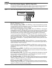
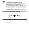
Data is transferred across the SDATA input/output pin. Data is driven on the falling edge
of SCLK and latched on the rising edge of SCLK. The least-significant bit of the data is
shifted first for both transmit and receive operations. During write operations, the processor
holds data for one-half of an SCLK period following the transfer of the last data bit. SDATA
has a weak keeper that holds the last value of SDATA on the pin.
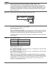
12.2 PROGRAMMABLE REGISTERS
The registers documented on the following pages are accessible to the system programmer.