Synchronous Serial Interface
12-4
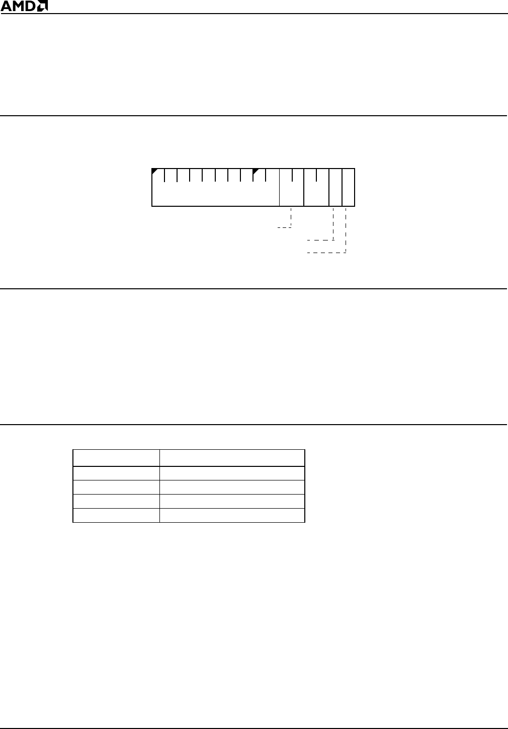
12.2.2 Synchronous Serial Control Register (SSC, Offset 12h)
This read/write register controls the operation of the SDEN0–SDEN1 outputs and the
transfer rate of the SSI port. The SDEN0 and SDEN1 outputs are asserted when a 1 is
written to the corresponding bit. However, in the case when both DE0 and DE1 are set,
only SDEN0 will be asserted. The format of the Synchronous Serial Control register is
shown in Figure 12-2.
Figure 12-2 Synchronous Serial Control Register (SSC, offset 12h)
The value of the SSC register at reset is 0000h.
Bits 15–6: Reserved—Set to 1.
Bits 5–4: SCLK Divide (SCLKDIV)—These bits determine the SCLK frequency. SCLK is
derived from the internal processor clock by dividing by 2, 4, 8, or 16. Table 12-2 shows
the processor clock frequency divider values for the possible SCLKDIV settings.
If power-save mode is in effect, the SCLK frequency is affected by the reduced processor
clock frequency.
Table 12-2 SCLK Divider Values
Bits 3–2: Reserved—Set to 0.
Bit 1: SDEN1 Enable (DE1)—When this bit is set to 1, the SDEN1 pin is held High. When
DE1 is set to 0, the SDEN1 pin is Low.
Bit 0: SDEN0 Enable (DE0)—When this bit is set to 1, the SDEN0 pin is held High. When
DE0 is set to 0, the SDEN0 pin is Low.
Note: The synchronous serial interface pins SDEN1–SDEN0, SCLK, and SDATA are
multiplexed with programmable I/O pins. To enable the pins to function as synchronous
serial interface, the PIO mode and PIO direction settings for the SDEN1–SDEN0, SCLK,
and SDATA pins must be set to 0 for normal operation. For more information, see
Chapter 13, “Programmable I/O Pins.”
SCLKDIV SCLK Frequency Divider
00b Processor clock / 2
01b Processor clock / 4
10b Processor clock / 8
11b Processor clock / 16
15
70
Reserved
SCLKDIV
DE1
DE0
Res


