Features and Performance
1-7
1.3.2 Memory Interface
The integrated memory controller logic of the Am186ER and Am188ER microcontrollers
provides a direct address bus interface to memory devices. The use of an external address
latch controlled by the address latch enable (ALE) signal is not required.
Individual byte write-enable signals are provided to eliminate the need for external high/
low-byte, write-enable circuitry. The maximum bank size programmable for the memory
chip-select signals is increased to 512 Kbyte to facilitate the use of high-density memory
devices.
Improved memory timing specifications enable the use of zero-wait-state memories with
70-ns access times at 40-MHz CPU operation. This reduces overall system cost
significantly by allowing the use of commonly available memory devices. The integrated
32-Kbyte RAM operates at the same speed as zero-wait-state external memory.
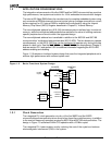
Figure 1-3 illustrates an Am186ER microcontroller-based configuration with 512 Kbyte of
external Flash EPROM in addition to the internal 32-Kbyte memory. Additional external
RAM can also be added. The external memory interface requires the following:
n The processor A19–A0 bus connects to the memory address inputs.
n The AD bus connects directly to the data inputs/outputs.
n The UCS chip select connects to the memory chip-select input.
External read operations require that the RD
output connects to the SRAM Output Enable
(OE
) input pin. External write operations require that the byte write enables connect to the SRAM
Write Enable (WE
) input pin.
The example design shown in Figure 1-3 uses a 4-Mbit (256-K x 16) external Flash EPROM
for application memory, mapped into the upper region of the microcontroller’s 1-Mbyte
address space at 80000h–FFFFFh. After a valid reset, the Am186ER or Am188ER
microcontroller will fetch the first instruction from address FFFF0h. The user application
can then enable and configure the location of the integrated 32-Kbyte RAM within the
remaining address space; in this example, it would be at address 00000h to accommodate
the interrupt vector table.
1.3.3 Serial Communications Port
The integrated universal asynchronous receiver/transmitter (UART) controller in the
Am186ER and Am188ER microcontrollers eliminates the need for external logic to
implement a communications interface. The integrated UART generates the serial clock
from the CPU clock so that no external time-base oscillator is required.
Figure 1-3 shows a minimal implementation of an RS-232 console or modem
communications port. The RS-232 to CMOS voltage-level converter is required for the
proper electrical interface with the external device.
The Am186ER and Am188ER microcontrollers also include a synchronous serial interface.
For more information, see Chapter 11.


