


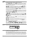

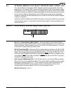


Internal Memory
6-2
6.3 EMULATOR AND DEBUG MODES
There are two debug modes associated with the internal memory. One mode allows users
to disable the internal RAM, and the other mode makes it possible to drive data on the
external data bus during internal RAM read cycles.
Normal operation of internal RAM has all control signals for reads and writes and data for
writes visible externally. Accesses to internal memory can be detected externally by
comparing the address on A19–A0 with the address space of the internal memory.
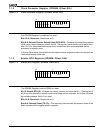
6.3.1 Internal Memory Disable
When this mode is activated, the internal RAM is disabled and all accesses into the internal
memory space are made externally for debugging purposes. This mode is activated by
pulling the S
1/IMDIS pin Low during reset. To use this debug mode, internal memory space
must first be activated via the IMCS Register as described on page 6-3.
6.3.2 Show Read Enable
When this mode is activated, the data from the internal RAM read cycles are driven on the
AD15–AD0 bus. Note that if a byte read is being shown, the unused byte will also be driven
on the AD15–AD0 bus. This mode can be activated externally by pulling the S
0/SREN pin
Low during reset or by setting the SR bit in the IMCS Register. If this feature is activated
externally using the SREN
pin, the value of the SR bit is ignored. Many emulators assert
the SREN
pin. For more details, see the IMCS Register information on page 6-3.
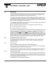
During an internal memory read with show read enabled, the address will be driven on the
AD bus during t
1
and t
2
. The data being read will be driven on the AD bus during t
3
and t
4
by the Am186ER or Am188ER microcontrollers. Special system care must be taken to
avoid bus contention, since normal reads have the AD bus three-stated during t
2
, t
3
, and
t
4
. It is best to ensure that no external device overlaps the internal memory space.