


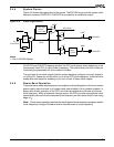


Peripheral Control Block
4-7
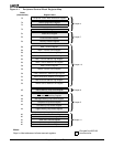
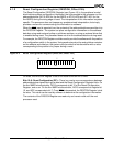
4.1.4 Power-Save Control Register (PDCON, Offset F0h)
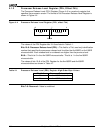
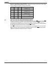
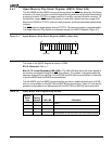
Figure 4-5 Power-Save Control Register (PDCON, offset F0h)
The value of the PDCON Register is 0000h at reset.
Bit 15: Enable Power-Save Mode (PSEN)—When set to 1, enables Power-Save mode
and divides the internal operating clock by the value in F2–F0. PSEN is automatically
cleared when an external interrupt occurs, including those generated by on-chip peripheral
devices. The value of the PSEN bit is not restored by the execution of an IRET instruction.
Software interrupts (INT instruction) and exceptions do not clear the PSEN bit, and interrupt
service routines for these conditions should do so if desired. This bit is 0 after processor
reset.
Bits 14–12: Reserved—Read back as 0.
Bit 11: CLKOUTB Output Frequency (CBF)—When set to 1, CLKOUTB follows the crystal
input (PLL) frequency. When set to 0, CLKOUTB follows the internal processor frequency
(after the clock divisor). Set to 0 on reset.
CLKOUTB can be used as a full-speed clock source in Power-Save mode.
Bit 10: CLKOUTB Drive Disable (CBD)—When set to 1, CBD three-states the clock output
driver for CLKOUTB. When set to 0, CLKOUTB is driven as an output. Set to 0 on reset.
Bit 9: CLKOUTA Output Frequency (CAF)—When set to 1, CLKOUTA follows the crystal
input (PLL) frequency. When set to 0, CLKOUTA follows the internal processor frequency
(after the clock divisor). Set to 0 on reset.
CLKOUTA can be used as a full-speed clock source in Power-Save mode.
Bit 8: CLKOUTA Drive Disable (CAD)—When set to 1, CAD three-states the clock output
driver for CLKOUTA. When set to 0, CLKOUTA is driven as an output. Set to 0 on reset.
Bits 7–3: Reserved—Read back as 0.
15
70
000 00000
CBD
CAF
CAD
F1
F0
F2
PSEN
CBF