System Overview
3-15
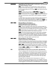
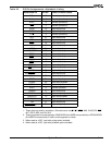
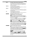
TMRIN1 Timer Input 1 (input, synchronous, edge-sensitive)
This pin supplies a clock or control signal to the internal microcontroller
timer 1. After internally synchronizing a Low-to-High transition on
TMRIN1, the microcontroller increments the timer. TMRIN1 must be
tied High if not being used.
TMROUT0 Timer Output 0 (output, synchronous)
This pin supplies the system with either a single pulse or a continuous
waveform with a programmable duty cycle.
TMROUT1 Timer Output 1 (output, synchronous)
This pin supplies the system with either a single pulse or a continuous
waveform with a programmable duty cycle. It can also be programmed
as a watchdog timer.
TXD Transmit Data (output, asynchronous)
This pin supplies asynchronous serial transmit data to the system from
the internal UART of the microcontroller.
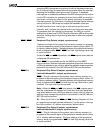
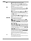
UCS
/ONCE1 Upper Memory Chip Select (output, synchronous)
ONCE Mode Request 1 (input, internal pullup)
UCS
—This pin indicates to the system that a memory access is in
progress to the upper memory block. The base address and size of the
upper memory block are programmable up to 512 Kbyte. UCS
is held
High during a bus hold condition.
After power-on reset, UCS
is asserted because the processor begins
executing at FFFF0h and the default configuration for the UCS
chip
select is 64 Kbyte from F0000h to FFFFFh. See section 5.5.1.
ONCE
1—During reset, this pin and ONCE0 indicate to the
microcontroller the mode in which it should operate. ONCE
0 and
ONCE
1 are sampled on the rising edge of RES. If both pins are asserted
Low, the microcontroller enters ONCE mode; otherwise, it operates
normally. In ONCE mode, all pins assume a high-impedance state and
remain in that state until a subsequent reset occurs. To guarantee that
the microcontroller does not inadvertently enter ONCE mode, ONCE
1
has a weak internal pullup resistor that is active only during a reset.
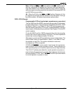
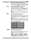
UZI
/CLKSEL2 Upper Zero Indicate (output, synchronous)
UZI
—This pin lets the designer determine whether an access to the
interrupt vector table is in progress by ORing it with bits 15–10 of the
address and data bus (AD15–AD10 on the Am186ER microcontroller
and AO15–AO10 on the Am188ER microcontroller). UZI
/CLKSEL2 is
the logical AND of the inverted A19–A16 bits, and it asserts in the first
period of a bus cycle and is held throughout the cycle.
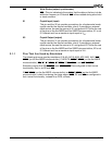
UZI
/CLKSEL2 is three-stated during bus holds and ONCE mode.
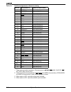
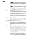
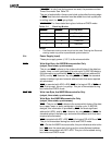
CLKSEL
2—The clocking mode of the Am186ER and Am188ER
microcontrollers is controlled by UZI
/CLKSEL2 and S6/CLKSEL1
during reset. Both CLKSEL
2 and CLKSEL1 are held High during power-
on reset because of an internal pullup resistor. The default clocking
mode—Times Four—is used if neither clock select is asserted Low
during reset.


