


System Overview
3-13
S2 Bus Cycle Status (output, three-state, synchronous)
S
2—This pin indicates to the system the type of bus cycle in progress.
S
2 can be used as a logical memory or I/O indicator. S2–S0 are three-stated
during bus holds, hold acknowledges, and ONCE mode. During reset,
these pins are pullups. The S
2–S0 pins are encoded as shown in Table 3-3.
S
1/IMDIS Bus Cycle Status (output, three-state, synchronous)
Internal Memory Disable (input, internal pullup)
S
1—This pin indicates to the system the type of bus cycle in progress.
S
1 can be used as a data transmit or receive indicator. S2–S0 are three-
stated during bus holds, hold acknowledges, and ONCE mode. During
reset, these pins are pullups. The S
2–S0 pins are encoded as shown in
Table 3-3.
IMDIS
—If asserted during reset, this pin disables internal memory.
Internal Memory Disable mode is provided for emulation and debugging
purposes.
S
0/SREN Bus Cycle Status (output, three-state, synchronous)
Show Read Enable (input, internal pullup)
S
0—This pin indicates to the system the type of bus cycle in progress.
S
2–S0 are three-stated during bus holds, hold acknowledges, and ONCE
mode. During reset, these pins are pullups. The S
2–S0 pins are encoded
as shown in Table 3-3.
SREN
—If asserted during reset, this pin enables data read from internal
memory to be shown/driven on the AD15–AD0 bus. Note that if a byte
read is being shown, the unused byte will also be driven on the AD15–
AD0 bus.This mode is provided for emulation and debugging purposes.
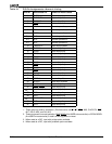
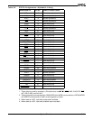
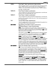
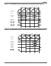
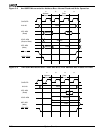
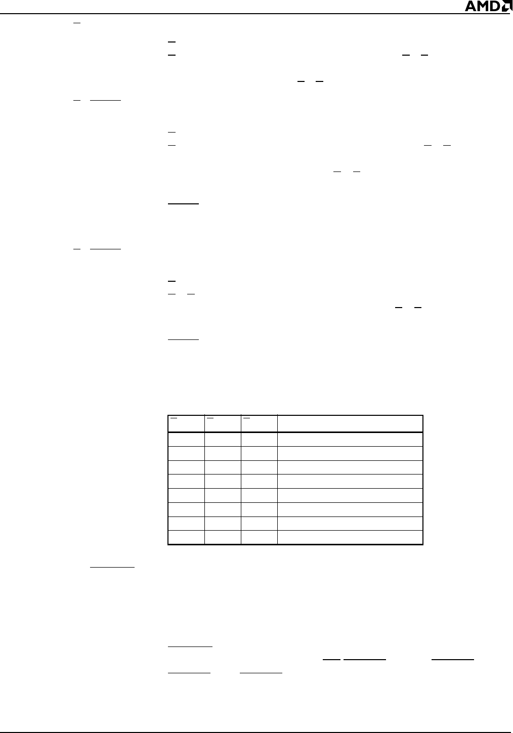
Table 3-3 Bus Cycle Encoding
S6/CLKSEL1 Bus Cycle Status Bit 6 (output, synchronous)
Clock Select 1 (input, internal pullup)
S6—During the second and remaining periods of a cycle (t
2
, t
3
, and t
4
),
this pin is asserted High to indicate a DMA-initiated bus cycle. During
a bus hold or reset condition, S6 is three-stated.
CLKSEL
1—The clocking mode of the Am186ER and Am188ER
microcontrollers is controlled by UZI
/CLKSEL2 and S6/CLKSEL1. Both
CLKSEL
2 and CLKSEL1 are held High during power-on reset because
of an internal pullup resistor. The default clocking mode—Times Four—
is used if neither clock select is asserted Low during reset.
S2S1S0 Bus Cycle
0 0 0 Interrupt acknowledge
0 0 1 Read data from I/O
0 1 0 Write data to I/O
011Halt
1 0 0 Instruction fetch
1 0 1 Read data from memory
1 1 0 Write data to memory
1 1 1 None (passive)