


Internal Memory
6-3
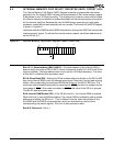
6.4 INTERNAL MEMORY CHIP SELECT REGISTER (IMCS, OFFSET ACh)
The Internal Memory Chip Select (IMCS) Register provides programmable chip select
generation for the internal RAM. It allows the base address of the internal memory space
to be placed on any 32-Kbyte boundary. The register also contains a control bit to enable
the internal memory and another to enable data read from the internal memory to be driven
on the external data bus. Because the internal RAM always executes zero-wait-state
accesses, a ready bit and wait-state bits are not included. The format of the IMCS Register
is shown in Figure 6-1.
Unlike the other Am186ER and Am188ER chip selects, writing to the IMCS will not activate
internal memory space. To activate the internal memory space, set a base address and
set the RE bit to 1.
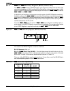
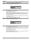
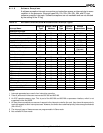
Figure 6-1 Internal Memory Chip Select Register (IMCS, offset ACh)
Bits 15–11: Base Address (BA19–BA15)—The base address of the internal RAM is
determined by the value of BA19–BA15, which corresponds to bits A19–A15 of the 20-bit
memory address. The base address can only be set on a 32-Kbyte boundary. The value
of this field is undefined after processor reset.
Bit 10: Show Read (SR)—Setting the SR bit enables data to be driven on the AD15–AD0
bus during internal RAM cycles for debugging purposes. Note that if a byte read is being
shown, the corresponding unused byte will also be driven on the AD15–AD0 bus. This
mode can also be enabled externally by asserting the SREN
pin which is sampled on the
rising edge of RES
. If this mode is enabled via SREN, the value of the SR bit is ignored.
This bit is 0 after processor reset.
Bit 9: Internal RAM Enable (RE)—If the RE bit is set to 1, the internal RAM is enabled.
When this bit is 0, internal RAM is disabled. The internal RAM is enabled by setting a base
address and setting the RE bit to 1. This is different from the other chip selects on the
Am186ER and Am188ER microcontrollers, which are activated by a write to their
corresponding chip select register. This bit is 0 after processor reset.
Bits 8–0: Reserved—Set to 1.
111111111
15
70
BA19–BA13
RE
SR