


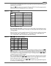


Chip Select Unit
5-9
be active in this case. Use of the MCS chip selects to access low memory allows the timing
of these accesses to follow the AD address bus rather than the A address bus. Locating a
512K MMCS block at 80000h always conflicts with the range of the UCS
chip select and
is not allowed.
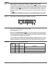
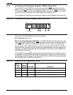
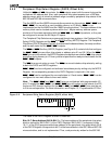
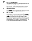
Bits 8–3: Reserved—Set to 1.
Bit 2: Ready Mode (R2)—The R2 bit is used to configure the Ready mode for the MCS
chip selects. If R2 is set to 0, external ready is required. If R2 is set to 1, external ready is
ignored. In each case, the processor also uses the value of the R1–R0 bits to determine
the number of wait states to insert.
Bits 1–0: Wait-State Value (R1–R0)—The value of R1–R0 determines the number of wait
states inserted into an access to the MCS
memory area. From zero to three wait states
can be inserted (R1–R0 = 00b to 11b).