Chip Select Unit
5-4
5.5.1 Upper Memory Chip Select Register (UMCS, Offset A0h)
The Am186ER and Am188ER microcontrollers provide the UCS chip select pin for the top
of memory. On reset, the microcontroller begins fetching and executing instructions starting
at memory location FFFF0h, so upper memory is usually used as instruction memory. To
facilitate this usage, UCS
defaults to active on reset with a default memory range of 64
Kbyte from F0000h to FFFFFh, external ready required, and three wait states automatically
inserted.
The UCS
memory range always ends at FFFFFh. The lower boundary is programmable.
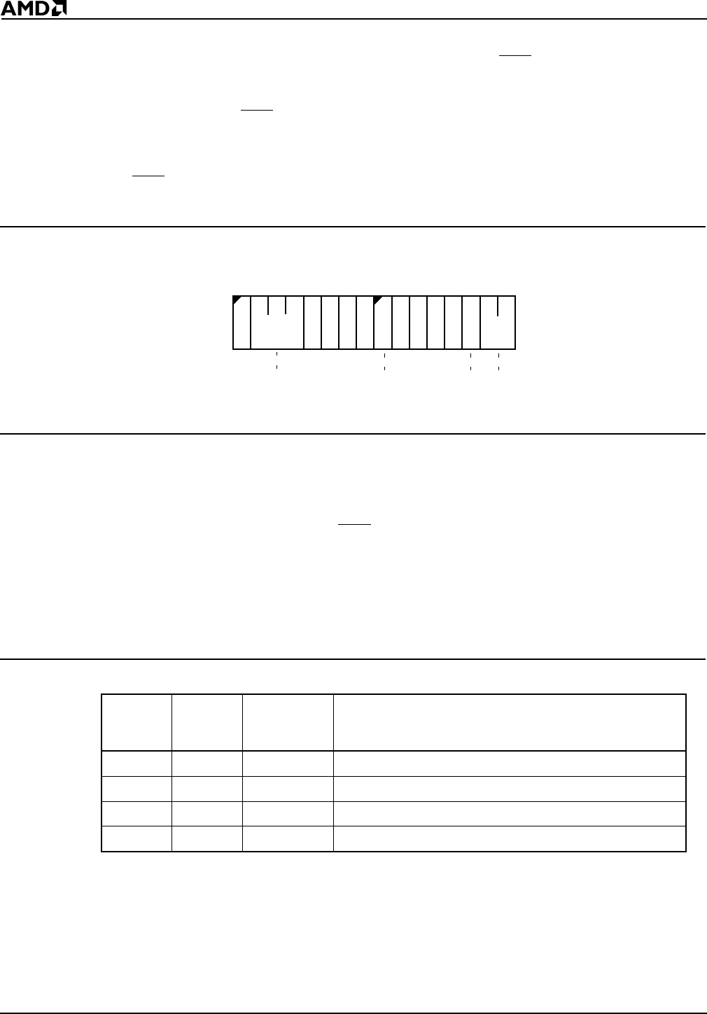
The Upper Memory Chip Select is configured through the UMCS Register (Figure 5-1).
Figure 5-1 Upper Memory Chip Select Register (UMCS, offset A0h)
The value of the UMCS Register at reset is F03Bh.
Bit 15: Reserved—Set to 1.
Bits 14–12: Lower Boundary (LB2–LB0)—The LB2–LB0 bits define the lower bound of
the memory accessed through the UCS
chip selects. The number of programmable bits
has been reduced from eight bits in the 80C186 and 80C188 microcontrollers to three bits
in the Am186ER and Am188ER microcontrollers.
The Am186ER and Am188ER microcontrollers provide an additional block size of 512K,
which is not available on the 80C186 and 80C188 microcontrollers. Table 5-2 outlines the
possible configurations and differences with the 80C186 and 80C188 microcontrollers.
Table 5-2 UMCS Block Size Programming Values
Memory
Block
Size
Starting
Address LB2–LB0 Comments
64K F0000h 111b
Default
128K E0000h 110b
256K C0000h 100b
512K 80000h 000b
Not available on the 80C186 or 80C188 microcontroller
15
70
LB2–LB0
10000
R1–R0
0
A19
111
R2DA


