


System Overview
3-3
AO8 and AD7–AD0 for the Am188ER microcontroller). The address is
guaranteed to be valid on the trailing edge of ALE. This pin is three-
stated during ONCE mode.
ARDY Asynchronous Ready (input, asynchronous, level-sensitive)
This pin indicates to the microcontroller that the addressed memory
space or I/O device will complete a data transfer. The ARDY pin accepts
a rising edge that is asynchronous to CLKOUTA and is active High. The
falling edge of ARDY must be synchronized to CLKOUTA. To always
assert the ready condition to the microcontroller, tie ARDY High. If the
system does not use ARDY, tie the pin Low to yield control to SRDY.
BHE
/ADEN Bus High Enable, Am186ER Microcontroller Only
(three-state, output, synchronous)
Address Enable, Am186ER Microcontroller Only
(input, internal pullup)
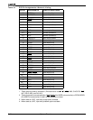
BHE
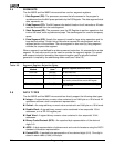
—During a memory access, this pin and the least significant
address bit (AD0 and A0) indicate to the system which bytes of the data
bus (upper, lower, or both) participate in a bus cycle. The BHE
/ADEN
and AD0 pins are encoded as shown in the following table.
BHE
is asserted during t
1
and remains asserted through t
3
and t
W
. BHE
does not need to be latched. BHE
is three-stated during bus hold and
reset conditions.
On the Am186ER microcontroller, WLB
and WHB implement the
functionality of BHE
and AD0 for high and low byte write enables.
BHE
/ADEN also signals DRAM refresh cycles when using the
multiplexed address and data (AD) bus. A refresh cycle is indicated
when both BHE
/ADEN and AD0 are High. During refresh cycles, the A
bus and the AD bus are not guaranteed to provide the same address
during the address phase of the AD bus cycle. For this reason, the A0
signal cannot be used in place of the AD0 signal to determine refresh
cycles. PSRAM refreshes also provide an additional RFSH
signal (see
the MCS
3/RFSH pin description).
ADEN
—If BHE/ADEN is held High or left three-stated during power-on
reset, the address portion of the AD bus (AD15–AD0) is enabled or
disabled during LCS
and UCS bus cycles based on the DA bit in the
Upper Memory Chip Select (UMCS) and Low Memory Chip Select
(LMCS) registers. If the DA bit is set, the memory address is accessed
on the A19–A0 pins. This mode of operation reduces power
consumption.
If BHE
/ADEN is held Low on power-on reset, the AD bus always drives
both addresses and data. (S6 and UZI also assume their normal
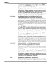
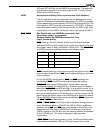
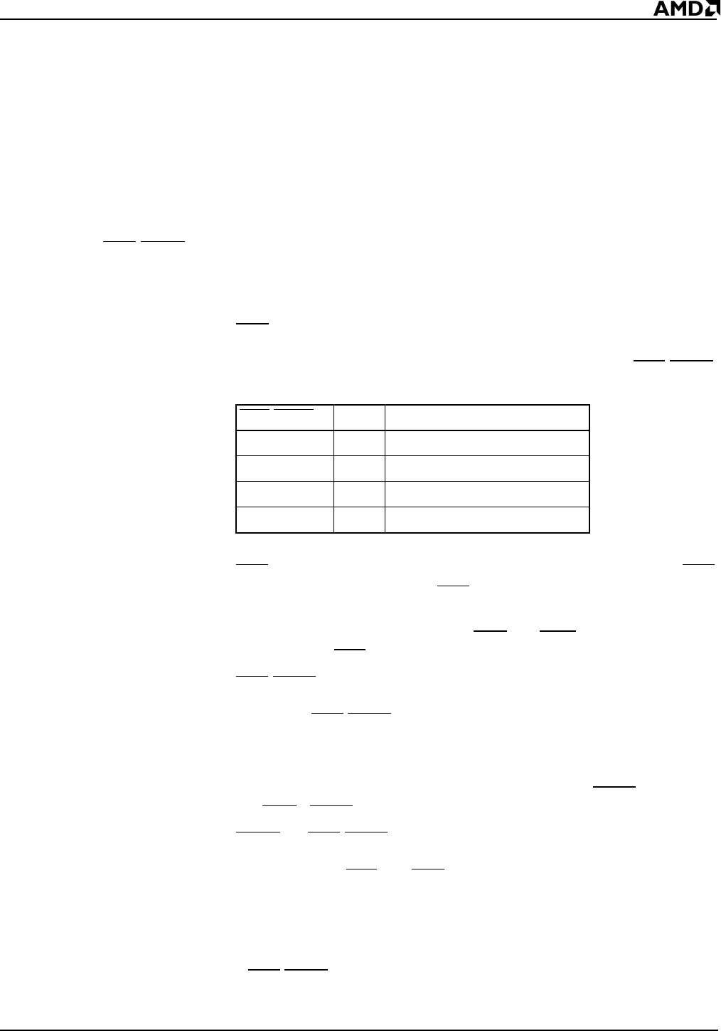
BHE/ADEN AD0 Type of Bus Cycle
0 0 Word Transfer
01High Byte Transfer (Bits 15–8)
1 0 Low Byte Transfer (Bits 7–0)
11Refresh