


Interrupt Control Unit
8-18
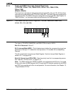
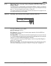
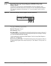
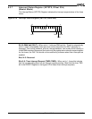
8.3.4 Timer and DMA Interrupt Control Registers
(TCUCON, Offset 32h, DMA0CON, Offset 34h, DMA1CON,
Offset 36h)
(Master Mode)
The three timer interrupts are assigned to interrupt types 08h, 12h, and 13h. All three timer
interrupts are configured through TCUCON, offset 32h. The DMA0 interrupt is assigned to
interrupt type 0Ah. The DMA1 interrupt is assigned to interrupt type 0Bh. See Chapter 10,
“DMA Controller,” for information about using these pins for DMA requests.
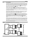
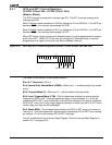
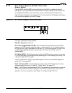
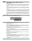
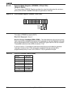
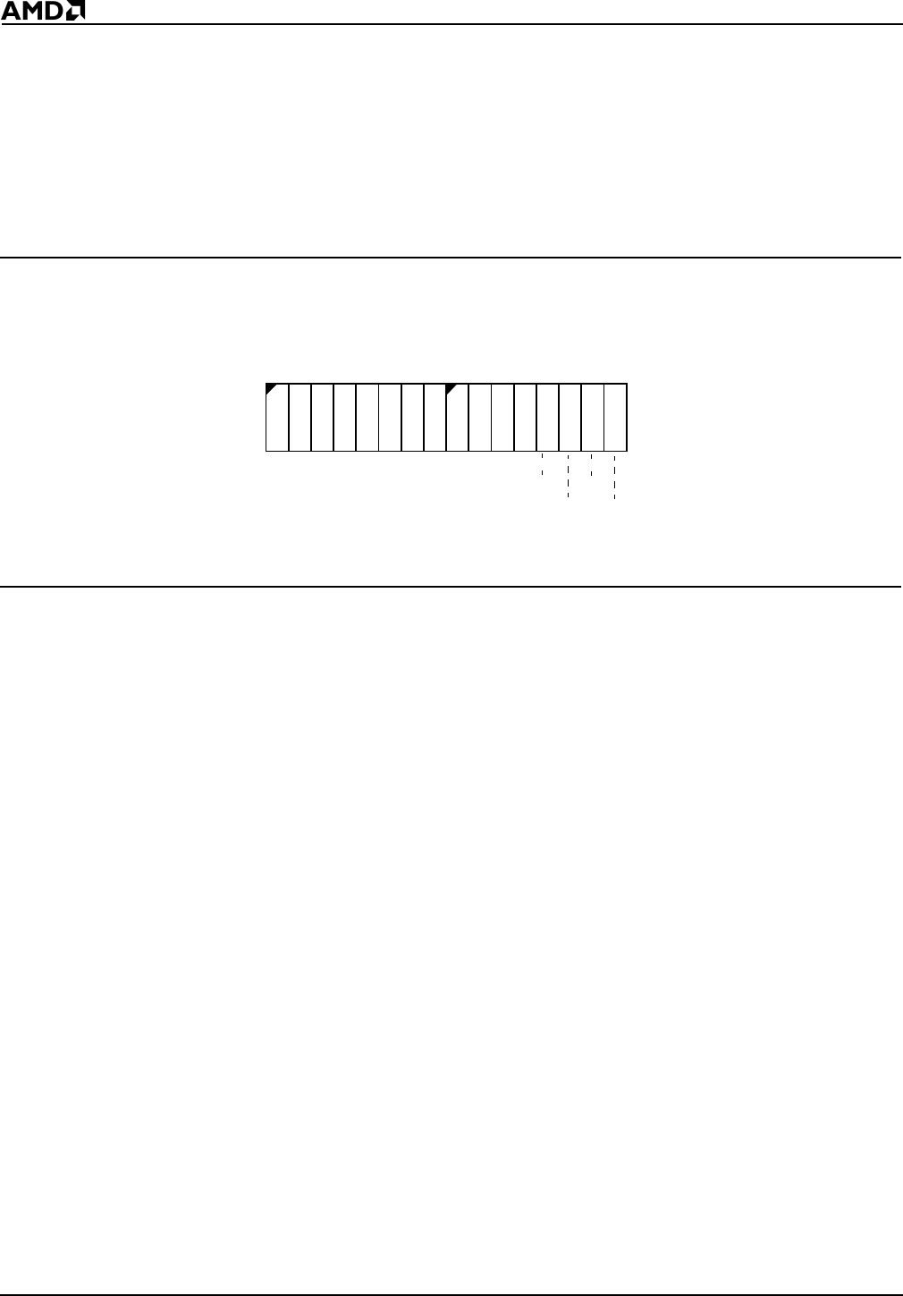
Figure 8-7 Timer/DMA Interrupt Control Registers (TCUCON, DMA0CON, DMA1CON,
offsets 32h, 34h, and 36h)
The value of TCUCON, DMA0CON, and DMA1CON at reset is 000Fh.
Bits 15–4: Reserved—Set to 0.
Bit 3: Interrupt Mask (MSK)—This bit determines whether the corresponding signal can
generate an interrupt. A 1 masks this interrupt source. A 0 enables the corresponding
interrupt.
This bit is duplicated in the Interrupt Mask Register. See the Interrupt Mask Register in
section 8.3.11 on page 8-25.
Bits 2–0: Priority Level (PR2–PR0)—Sets the priority level for its corresponding source.
See Table 8-3, “Priority Level,” on page 8-15.
Note: The DMA request pins DRQ0 and DRQ1 are multiplexed with PIO pins. To enable
the pins to function as DMA request, the PIO mode and PIO direction settings for the DRQ0
and DRQ1 pins must be set to 0 for normal operation. For more information, see Chapter 13,
“Programmable I/O Pins.”
15
70
000 000 000000
PR2
PR1
PR0
MSK