


Internal Memory
6-1
CHAPTER
6
INTERNAL MEMORY
6.1 OVERVIEW
The Am186ER and Am188ER microcontrollers provide 32 Kbyte of on-chip RAM. The
integration of memory helps reduce a system design’s overall cost, size, and power
consumption.
The internal RAM for the Am186ER microcontroller is a 16K x 16-bit-wide array, which
provides the same performance as 16-bit external zero-wait-state RAM. The internal RAM
for the Am188ER microcontroller is a 32K x 8-bit-wide array, which provides the same
performance as 8-bit external zero-wait-state RAM.
6.2 INTERACTION WITH EXTERNAL RAM
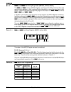
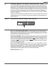
The Am186ER and Am188ER microcontrollers include an Internal Memory Chip Select
(IMCS) Register to enable and control the mapping of the internal RAM. For a detailed
description of the IMCS Register, see “Internal Memory Chip Select Register (IMCS, Offset
ACh)” on page 6-3.
The IMCS Register can be configured to locate the internal address space at any 32-Kbyte
boundary within the 1-Mbyte memory address space. The base address is determined by
the value of bits BA19–BA15 in the IMCS Register.
If the internal memory overlaps with an external memory chip select, the external memory
chip select must be set to zero wait states with no external ready required. If internal and
external chip selects overlap, both will be active, but the internal memory data will be used
on reads. Writes, with all the corresponding external control signals, will occur to both
devices. Special system consideration must be made if the show read enable feature
described on page 6-2 is used, because that feature drives data to the external bus during
internal memory read cycles.
If internal and external chip selects overlap and the external chip selects are
not
set to zero
wait states with no external ready required, the results are unpredictable. Note that because
of the many potential problems with overlapping chip selects, this practice is not
recommended.
A memory overlap might be unavoidable in some designs, however. Because the interrupt
vector table is located at 00000h, it is not unusual to store the interrupt vector table in the
internal RAM for faster access, and thus program the IMCS Register for a base address
of 0. This situation could lead to a memory address overlap between the IMCS and low
memory chip select (LMCS) registers, as the base address of the LMCS Register is always
0 if activated. For more information about the LMCS Register, see “Low Memory Chip Select
Register (LMCS, Offset A2h)” on page 5-6.