


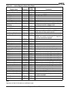

Peripheral Control Block
4-4
4.1.1 Peripheral Control Block Relocation Register (RELREG, Offset FEh)
The peripheral control block is mapped into either memory or I/O space by programming
the Peripheral Control Block Relocation (RELREG) Register (see Figure 4-2). This register
is a 16-bit register at offset FEh from the control block base address. The RELREG Register
provides the upper 12 bits of the base address of the control block. The control block is
effectively an internal chip select range.
Other chip selects can overlap the control block only if they are programmed to zero wait
states and ignore external ready. If the control register block is mapped into I/O space, the
upper four bits of the base address must be programmed as 0000b (because I/O addresses
are only 16 bits wide).
In addition to providing relocation information for the control block, the RELREG Register
contains a bit that places the interrupt controller into either Slave mode or Master mode.
At reset, the RELREG Register is set to 20FFh, which maps the control block to start at
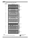
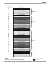
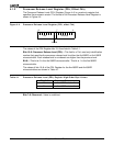
FF00h in I/O space. An offset map of the 256-byte peripheral control register block is shown
in Figure 4-1.
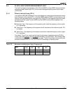
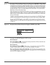
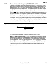
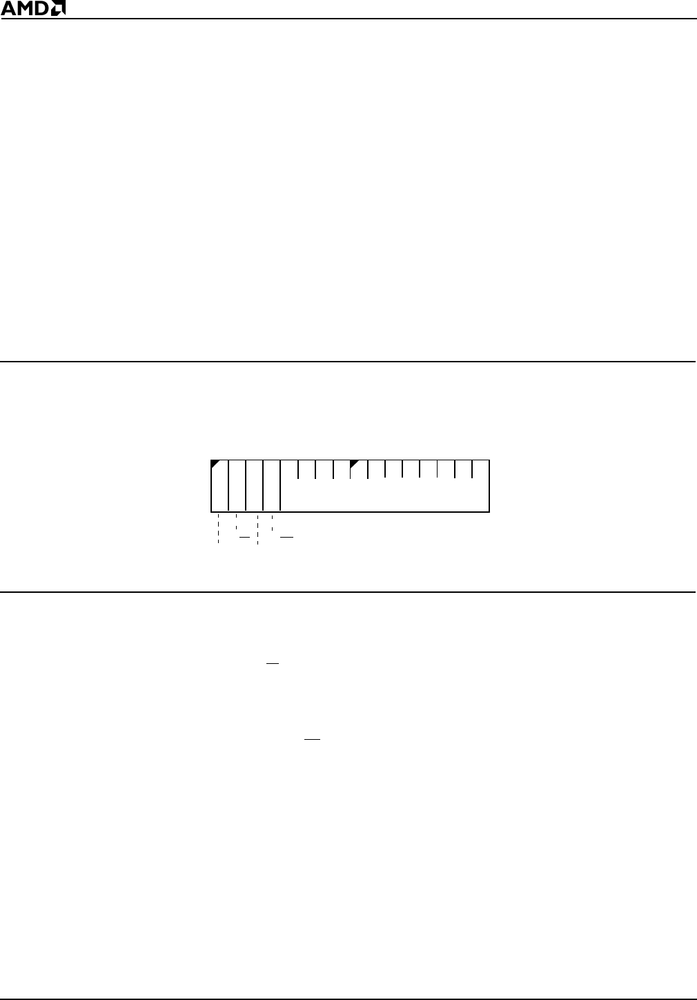
Figure 4-2 Peripheral Control Block Relocation Register (RELREG, offset FEh)
The value of the RELREG Register is 20FFh at reset.
Bit 15: Reserved
Bit 14: Slave/Master (S/M
)—Configures the interrupt controller for Slave mode when set
to 1 and for Master mode when set to 0.
Bit 13: Reserved
Bit 12: Memory/IO Space (M/IO
)—When set to 1, the peripheral control block (PCB) is
located in memory space. When set to 0, the PCB is located in I/O space.
Bits 11–0: Relocation Address Bits (R19–R8)—R19–R8 define the upper address bits
of the PCB base address. The lower eight bits (R7–R0) default to 00h. R19–R16 are ignored
when the PCB is mapped to I/O space.
15
70
Res
S/M
R19–R8
Res
M/IO