


Chip Select Unit
5-8
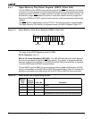
5.5.3 Midrange Memory Chip Select Register (MMCS, Offset A6h)
The Am186ER and Am188ER microcontrollers provide four chip select pins, MCS3–MCS0,
for use within a user-locatable memory block. The base address of the memory block can
be located anywhere within the 1-Mbyte memory address space, exclusive of the areas
associated with the UCS
and LCS chip selects (and, if they are mapped to memory, the
address range of the Peripheral Chip Selects, PCS
6–PCS5 and PCS3–PCS0). The MCS
address range can overlap the PCS
address range if the PCS chip selects are mapped to
I/O space.
The Midrange Memory Chip Selects are programmed through two registers. The Midrange
Memory Chip Select (MMCS) Register (see Figure 5-3) determines the base address and
the ready condition and wait states of the memory block accessed through the MCS
pins.
The PCS
and MCS Auxiliary (MPCS) Register is used to configure the block size. The
MCS
3–MCS0 pins are not active on reset. Both the MMCS and MPCS registers must be
accessed with a write to activate these chip selects.
Unlike the UCS
and LCS chip selects, the MCS3–MCS0 outputs assert with the multiplexed
AD address bus (AD15–AD0 or AO15–AO8 and AD7–AD0) rather than the earlier timing
of the A19–A0 bus. The A19–A0 bus can still be used for address selection, but the timing
is delayed for a half cycle later than that for UCS
and LCS.
Note: The MCS3–MCS0 pins are multiplexed with programmable I/O pins. To enable the
MCS
3–MCS0 pins to function as chip selects, the PIO mode and PIO direction settings for
the MCS
3–MCS0 pins must be set to 0 for normal operation. For more information, see
Chapter 13, “Programmable I/O Pins.”
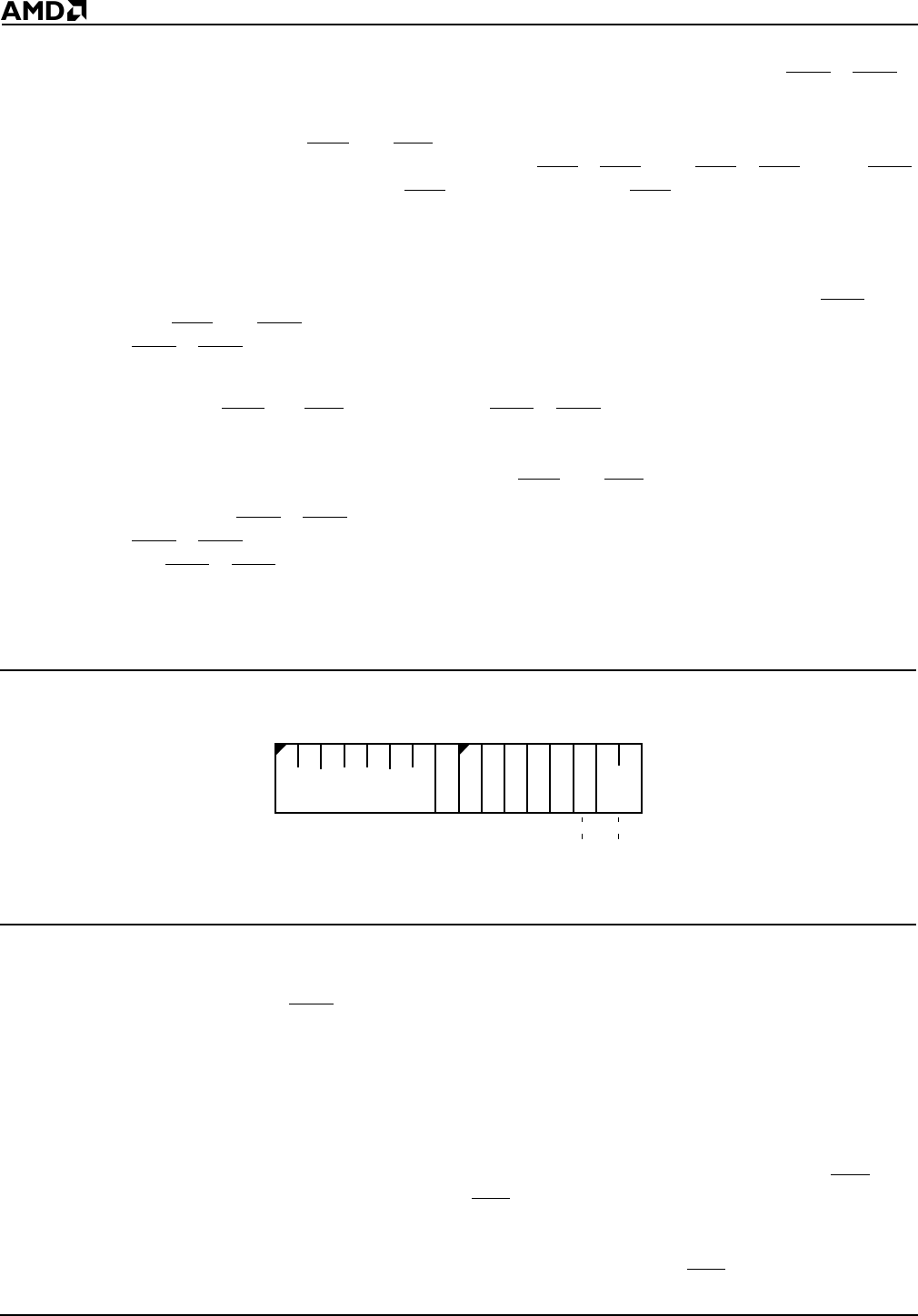
The Midrange Memory Chip Selects are configured by the MMCS Register (Figure 5-3).
Figure 5-3 Midrange Memory Chip Select Register (MMCS, offset A6h)
The value of the MMCS Register at reset is undefined.
Bits 15–9: Base Address (BA19–BA13)—The base address of the memory block that is
addressed by the MCS
chip select pins is determined by the value of BA19–BA13. These
bits correspond to bits A19–A13 of the 20-bit memory address. Bits A12–A0 of the base
address are always 0.
The base address can be set to any integer multiple of the size of the memory block size
selected in the MPCS Register. For example, if the midrange block is 32 Kbyte, the block
could be located at 10000h or 18000h but not at 14000h.
The base address of the midrange chip selects can be set to 00000h only if the LCS
chip
select is not active. This is because the LCS
base address is defined to be address 00000h
and chip select address ranges are not allowed to overlap. Because of the additional
restriction that the base address must be a multiple of the block size, a 512K MMCS block
size can only be used when located at address 00000h, and the LCS
chip selects must not
15
70
BA19–BA13 1 1 1111
R1–R0
R2