


System Overview
3-16
If CLKSEL2 is held Low during power-on reset, the processor enters
Times One mode. See Table 3-4.
This pin is latched within three crystal clock cycles after the rising edge
of RES
. Note that clock selection must be stable four clock cycles prior
to exiting reset (i.e., RES
going High).
UZI
/CLKSEL2 is three-stated during bus holds and ONCE mode.
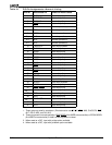
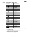
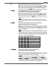
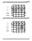
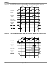
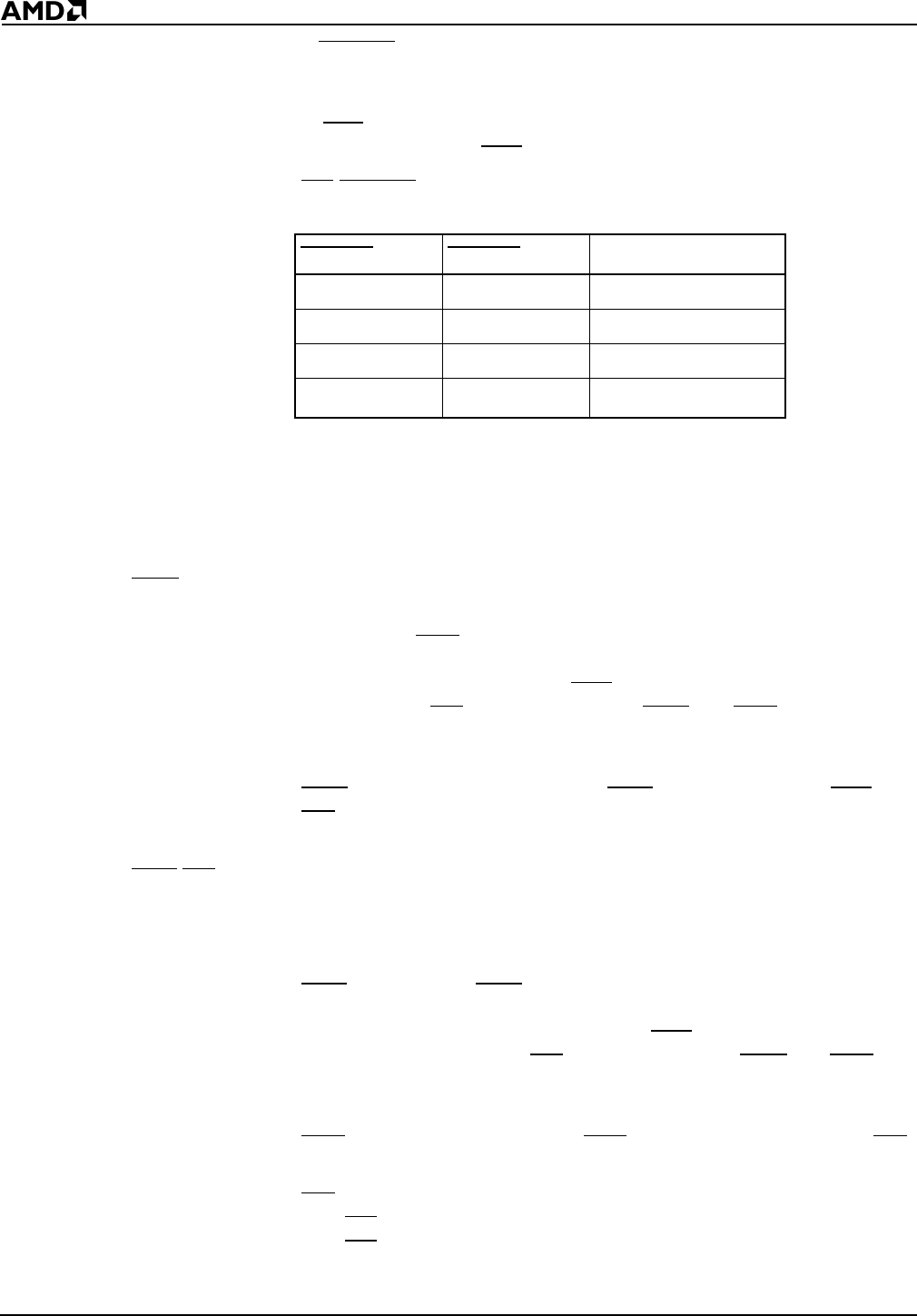
Table 3-4 Clocking Modes
Notes:
1 The Reserved clocking mode should not be used. Entering the Reserved
clocking mode may cause unpredictable system behavior.
V
CC
Power Supply (input)
These pins supply power (+3.3 V) to the microcontroller.
WHB
Write High Byte, Am186ER Microcontroller Only
(output, three-state, synchronous)
This pin and WLB
indicate to the system which bytes of the data bus
(upper, lower, or both) participate in a write cycle. In 80C186 designs,
this information is provided by BHE
, the least-significant address bit
(AD0), and by WR
. However, by using WHB and WLB, the standard
system-interface logic and external address latch that were required
are eliminated.
WHB
is asserted with AD15–AD8. WHB is the logical OR of BHE and
WR
. During reset, this pin is a pullup. This pin is three-stated during
bus holds and ONCE mode.
WLB
/WB Write Low Byte, Am186ER Microcontroller Only
(output, three-state, synchronous)
Write Byte, Am188ER Microcontroller Only
(output, three-state, synchronous)
WLB
—This pin and WHB indicate to the system which bytes of the data
bus (upper, lower, or both) participate in a write cycle. In 80C186
designs, this information is provided by BHE
, the least-significant
address bit (AD0), and by WR
. However, by using WHB and WLB, the
standard system interface logic and external address latch that were
required are eliminated.
WLB
is asserted with AD7–AD0. WLB is the logical OR of AD0 and WR.
This pin is three-stated during bus holds and ONCE mode.
WB
—On the Am188ER microcontroller, this pin indicates a write to the
bus. WB
uses the same early timing as the nonmultiplexed address
bus. WB
is associated with AD7–AD0. This pin is three-stated during
bus holds and ONCE mode.
CLKSEL2CLKSEL1 Clocking Mode
H H Times Four
HLDivide by Two
LHTimes One
LL
Reserved
1