Chip Select Unit
5-1
CHAPTER
5
CHIP SELECT UNIT
5.1 OVERVIEW
The Am186ER and Am188ER microcontrollers contain logic that provides programmable
chip select generation for both memories and peripherals. In addition, the logic can be
programmed to provide ready or wait-state generation and latched address bits A1 and A2.
The chip select lines are active for all memory and I/O cycles in their programmed areas,
whether they are generated by the CPU or by the integrated DMA unit.
The Am186ER and Am188ER microcontrollers provide six chip select outputs for use with
external memory devices and six more for use with peripherals in either memory space or
I/O space. The six memory chip selects can be used to address three memory ranges.
Each peripheral chip select addresses a 256-byte block offset from a programmable base
address (see section 4.1.1 on page 4-4).
The Am186ER and Am188ER microcontrollers also provide 32-Kbyte of internal memory,
described in Chapter 6. The Internal Memory Chip Select Register is described on page 6-3.
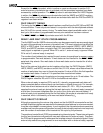
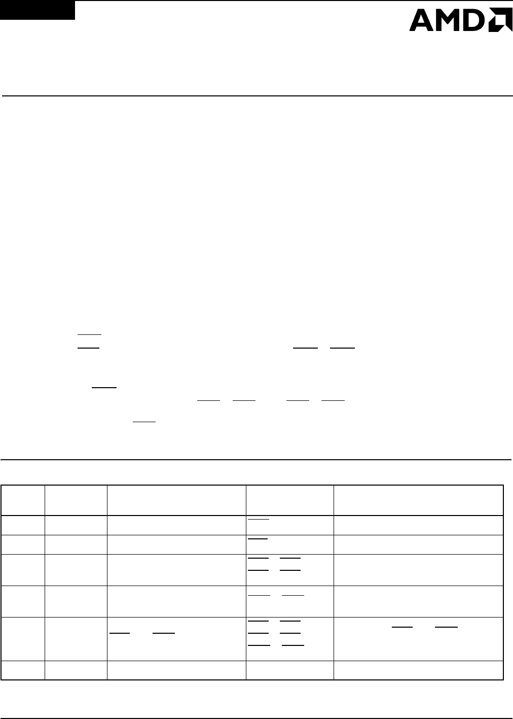
The chip selects are programmed through the use of five 16-bit peripheral registers (Table
5-1). The UMCS Register, offset A0h, is used to program the Upper Memory Chip Select
(UCS
). The LMCS Register, offset A2h, is used to program the Lower Memory Chip Select
(LCS
). The Midrange Memory Chip Selects (MCS3–MCS0) are programmed through the
use of two registers—the Midrange Memory Chip Select (MMCS) Register, offset A6h and
the PCS and MCS Auxiliary (MPCS) Register, offset A8h. In addition to its use in configuring
the MCS
chip selects, the MPCS Register and the PACS Register are used to program the
Peripheral Chip Selects (PCS
6–PCS5 and PCS3–PCS0).
Note: The PCS4 chip select is not implemented on the Am186ER and Am188ER
microcontrollers.
Table 5-1 Chip Select Register Summary
Note:
A write will enable an external memory or peripheral chip select register.
Offset
Register
Mnemonic Register Name Affected Pins Comments
A0h UMCS Upper Memory Chip Select UCS
Ending address is fixed at FFFFFh
A2h LMCS Lower Memory Chip Select LCS
Starting address is fixed at 00000h
A4h PACS Peripheral Chip Select
PCS
6–PCS5
PCS
3–PCS0
Block size is fixed at 256 bytes
A6h MMCS Midrange Chip Select MCS
3–MCS0
Starting address and block size are
programmable
A8h MPCS PCS
and MCS Auxiliary
PCS
6–PCS5
PCS
3–PCS0
MCS
3–MCS0
Affects both PCS
and MCS
chip selects
ACh IMCS Internal Memory Chip Select None. See Chapter 6, “Internal Memory.”


