


Chip Select Unit
5-10
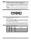
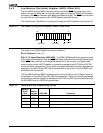
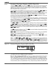
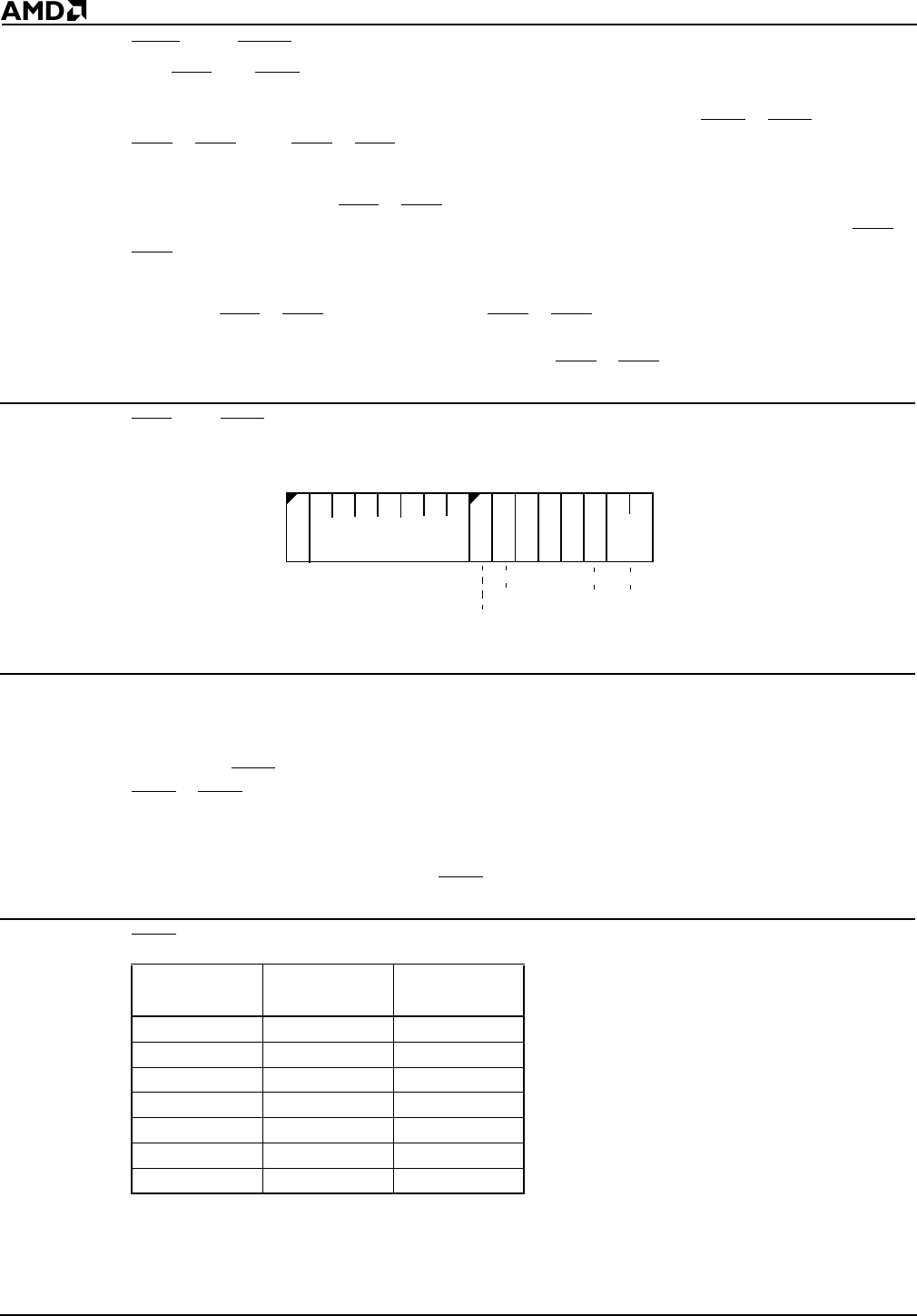
5.5.4 PCS and MCS Auxiliary Register (MPCS, Offset A8h)
The PCS and MCS Auxiliary (MPCS) Register (see Figure 5-4) differs from the other chip
select control registers in that it contains fields that pertain to more than one type of chip
select. The MPCS Register fields provide program information for MCS
3–MCS0 as well as
PCS
6–PCS5 and PCS3–PCS0.
In addition to its function as a chip select control register, the MPCS Register contains a
field that configures the PCS
6–PCS5 pins as either chip selects or as alternate sources for
the A2 and A1 address bits. When programmed to provide address bits A1 and A2, PCS
6–
PCS
5 cannot be used as peripheral chip selects. These outputs can be used to provide
latched address bits for A2 and A1.
On reset, PCS
6–PCS5 are not active. If PCS6–PCS5 are configured as address pins, a
write access to the MPCS Register causes the pins to activate. No corresponding access
to the PACS Register is required to activate the PCS
6–PCS5 pins as addresses.
Figure 5-4 PCS and MCS Auxiliary Register (MPCS, offset A8h)
The value of the MPCS Register at reset is undefined.
Bit 15: Reserved—Set to 1.
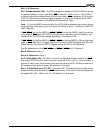
Bits 14–8: MCS
Block Size (M6–M0)—This field determines the total block size for the
MCS
3–MCS0 chip selects. Each individual chip select is active for one quarter of the total
block size. The size of the memory block defined is shown in Table 5-4.
Only one of the M6–M0 bits can be set at any time. If more than one of the M6–M0 bits is
set, unpredictable operation of the MCS
lines occurs.
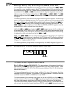
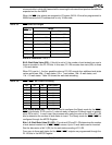
Table 5-4 MCS Block Size Programming
Total Block
Size
Individual
Select Size M6–M0
8K 2K 0000001b
16K 4K 0000010b
32K 8K 0000100b
64K 16K 0001000b
128K 32K 0010000b
256K 64K 0100000b
512K 128K 1000000b
15
70
MS
EX
M6–M0
1
11 1
R1–R0
R2