


DMA Controller
10-12
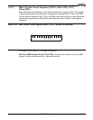
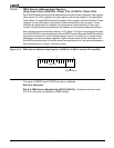
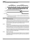
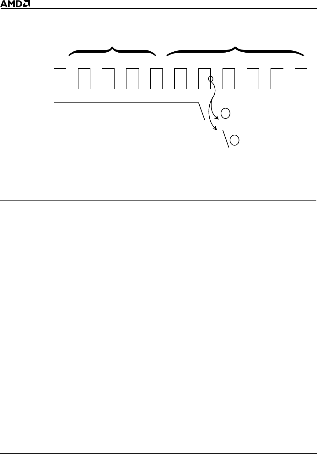
Figure 10-9 Destination Synchronized DMA Transfers
Notes:
1. This destination-synchronized transfer is not followed immediately by another DMA transfer.
2. This destination-synchronized transfer is immediately followed by another DMA transfer because
DRQ is not deasserted soon enough.
10.4.2 DMA Acknowledge
No explicit DMA acknowledge signal is provided. Because both source and destination
registers are maintained, a read from a requesting source or a write to a requesting
destination should be used as the DMA acknowledge signal. Because the chip-select lines
can be programmed to be active for a given block of memory or I/O space, and the DMA
source and destination address registers can be programmed to point to the same given
block, a chip-select line could be used to indicate a DMA acknowledge.
10.4.3 DMA Priority
The DMA channels can be programmed so that one channel is always given priority over
the other, or they can be programmed to alternate cycles when both have DMA requests
pending (see section 10.3.1, bit 5, the P bit). DMA cycles always have priority over internal
CPU cycles except between internally locked memory accesses or word accesses to odd
memory locations. However, an external bus hold takes priority over an internal DMA cycle.
Because an interrupt request cannot suspend a DMA operation and the CPU cannot access
memory during a DMA cycle, interrupt latency time suffers during sequences of continuous
DMA cycles. An NMI request, however, causes all internal DMA activity to halt. This allows
the CPU to respond quickly to the NMI request.
10.4.4 DMA Programming
DMA cycles occur whenever the ST bit of the control register is set. If synchronized transfers
are programmed, a DRQ must also be generated. Therefore, the source and destination
transfer address registers and the transfer count register (if used) must be programmed
before the ST bit is set.
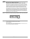
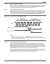
T1 T2 T3 T4 T1 T2 T3 T4
CLKOUT
DRQ
(First case)
DRQ
(Second case)
Fetch Cycle Deposit Cycle
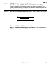
1
2
TI TI