


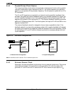


System Overview
3-22
The refresh control unit must be programmed before accessing PSRAM in LCS space. The
refresh counter in the Clock Prescaler (CDRAM) Register must be configured with the
required refresh interval value. The ending address of LCS space and the ready and wait-
state generation in the LMCS Register must also be programmed.
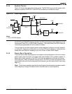
The refresh counter reload value in the CDRAM Register should not be set to less than 18
(12h) in order to provide time for processor cycles within refresh. In PSRAM mode, the
refresh address counter must be set to 0000h to prevent another chip select from asserting.
LCS
is held High during a refresh cycle. The A19–A0 bus is not used during refresh cycles.
The LMCS Register must be configured to external Ready ignored (R2=1) with one wait
state (R1–R0=01b), and the PSRAM mode enable bit (PSE) must be set to 1. See section
5.5.2 on page 5-6.