


Synchronous Serial Interface
12-6
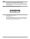
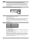
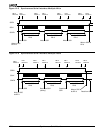
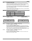
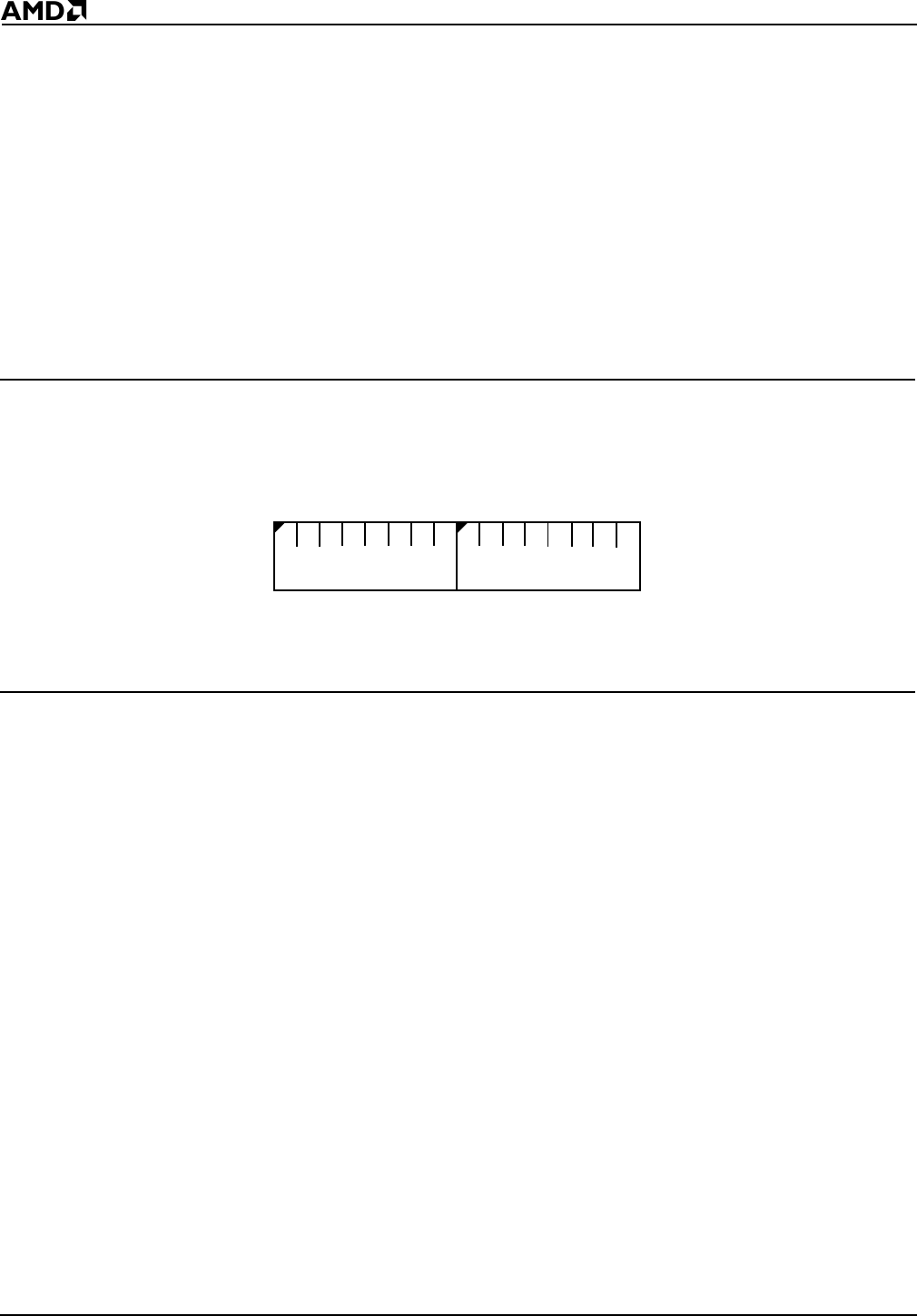
12.2.4 Synchronous Serial Receive Register (SSR, Offset 18h)
The Synchronous Serial Receive (SSR) register contains the data transferred from the
peripheral to the processor on a read operation. Only the least-significant 8 bits of the
register are used. The format of the SSR register is shown in Figure 12-4.
A receive data transmission is initiated by reading the SSR register while the port is not
busy (PB bit in SSS register is 0) and one or both of the enable bits (DE1–DE0 in the SSC
register) is set. A receive transmission is not initiated by reading the SSR register when
neither of the enable bits is set (DE1–DE0 = 00b). This allows the software to read the
received data without initiating another receive transmission.
A read of the Synchronous Serial Receive register while the port is busy (PB bit is set in
the SSS register) sets the RE/TE (Receive/Transmit Error) bit in the SSS register and
returns an indeterminate value. Such a read does not generate additional data transfers.
Figure 12-4 Synchronous Serial Receive Register (SSR, offset 18h)
The value of this register at reset is undefined.
Bits 15–8: Reserved—Set to 0.
Bits 7–0: Receive Data (SR)—Data received over the SDATA pin. Bit 0 is transmitted first,
bit 7 is transmitted last.
15
70
Reserved
SR