


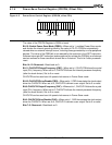


Chip Select Unit
5-5
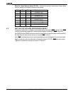
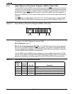
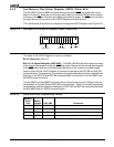
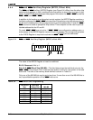
Bits 11–8: Reserved
Bit 7: Disable Address (DA)—The DA bit enables or disables the AD15–AD0 bus during
the address phase of a bus cycle when UCS
is asserted. If DA is set to 1, AD15–AD0 is
not driven during the address phase of a bus cycle when UCS
is asserted. If DA is set to
0, AD15–AD0 is driven during the address phase of a bus cycle. Disabling AD15–AD0
reduces power consumption. DA defaults to 0 at power-on reset.
Note: On the Am188ER microcontroller, the AO15–AO8 address pins are driven during
the data phase of the bus cycles, even when the DA bit is set to 1 in either the UMCS or
LMCS Register.
If BHE/ADEN (on the Am186ER) or RFSH2/ADEN (on the Am188ER) is held Low on the
rising edge of RES
, then AD15–AD0 is always driven regardless of the DA setting. This
configures AD15–AD0 to be enabled regardless of the setting of DA.
If BHE
/ADEN (on the Am186ER) or RFSH2/ADEN (on the Am188ER) is High on the rising
edge of RES
, then DA in the Upper Memory Chip Select (UMCS) Register and DA in the
Lower Memory Chip Select (LMCS) Register control the AD15–AD0 disabling.
See the descriptions of the BHE
/ADEN and RFSH2/ADEN pins in Chapter 3.
Bits 6: Reserved—Set to 0.
Bits 5–3: Reserved—Set to 1.
Bit 2: Ready Mode (R2)—The R2 bit is used to configure the Ready mode for the UCS
chip select. If R2 is set to 0, external ready is required. If R2 is set to 1, external ready is
ignored. In each case, the processor also uses the value of the R1–R0 bits to determine
the number of wait states to insert. R2 defaults to 0 at reset.
Bits 1–0: Wait-State Value (R1–R0)—The value of R1–R0 determines the number of wait
states inserted into an access to the UCS
memory area. From zero to three wait states can
be inserted (R1–R0 = 00b to 11b). R1–R0 default to 11b at reset.