


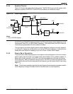


System Overview
3-21
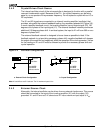
3.3 BUS INTERFACE UNIT
The bus interface unit controls all accesses to external peripherals and memory devices.
External accesses include those to memory devices, as well as those to memory-mapped
and I/O-mapped peripherals and the peripheral control block. The Am186ER and Am188ER
microcontrollers provide an enhanced bus interface unit with the following features:
n A nonmultiplexed address bus
n Separate byte write enables for high and low bytes in the Am186ER microcontroller
n Pseudo-static RAM (PSRAM) support
The standard 80C186 multiplexed address and data bus requires system-interface logic
and an external address latch. On the Am186ER and Am188ER microcontrollers, new byte
write enables, PSRAM control logic, and a new nonmultiplexed address bus can reduce
design costs by eliminating external logic.
Timing diagrams for the operations described in this chapter appear in the
Am186ER and
Am188ER Microcontrollers Data Sheet
, order #20732.
3.3.1 Nonmultiplexed Address Bus
The nonmultiplexed address bus (A19–A0) is valid one-half CLKOUTA cycle in advance
of the address on the AD bus. When used in conjunction with the modified UCS
and LCS
outputs and the byte write enable signals, the A19–A0 bus provides a seamless interface
to SRAM, PSRAM, and Flash/EPROM memory systems.
3.3.2 Byte Write Enables
The Am186ER microcontroller provides two signals that act as byte write enables—WHB
(Write High Byte, AD15–AD8) and WLB
(Write Low Byte, AD7–AD0). WHB is the logical
AND of BHE
and WR (WHB is Low when both BHE and WR are Low). WLB is the logical
AND of AD0 and WR
(WLB is Low when both AD0 and WR are both Low).
The Am188ER microcontroller provides one signal for byte write enables—WB
(Write Byte).
WB
is the logical AND of WHB and WLB, which are not present on the Am188ER
microcontroller.
The byte write enables are driven in conjunction with the demultiplexed address bus as
required for the write timing requirements of common SRAMs.
3.3.3 Pseudo Static RAM (PSRAM) Support
The Am186ER and Am188ER microcontrollers support the use of PSRAM devices in low
memory chip select (LCS) space only. When PSRAM mode is enabled, the timing for the
LCS
signal is modified by the chip select control unit to provide a CS precharge period
during PSRAM accesses. The 40-MHz timing of the Am186ER microcontroller is
appropriate to allow 70-ns PSRAM to run with one wait state. PSRAM mode is enabled
through a bit in the Low Memory Chip Select (LMCS) Register. (See section 5.5.2 on page
5-6.) The PSRAM feature is disabled on CPU reset.
In addition to the LCS
timing changes for PSRAM precharge, the PSRAM devices also
require periodic refresh of all internal row addresses to retain their data. Although refresh
of PSRAM can be accomplished several ways, the Am186ER and Am188ER
microcontrollers implement auto refresh only. The microcontroller generates a refresh
signal, RFSH
, to the PSRAM devices when PSRAM mode is enabled. No refresh address
is required by the PSRAM when using the auto refresh mechanism. The RFSH
signal is
multiplexed with the MCS
3 signal pin. When PSRAM mode is enabled, MCS3 is not
available for use as a chip select signal.