


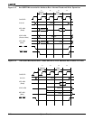

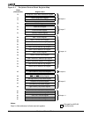
Peripheral Control Block
4-2
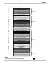
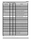
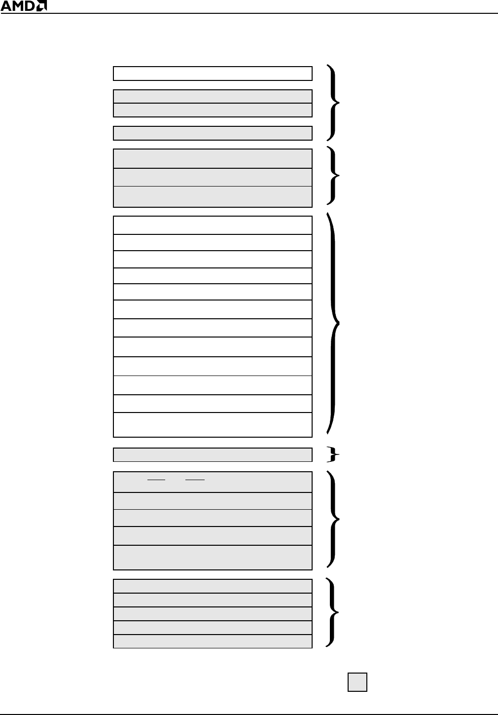
Figure 4-1 Peripheral Control Block Register Map
Chapter 4
Chapter 7
Chapter 10
Chapter 5
Chapter 11
PCS and MCS Auxiliary Register
A8
DA
Memory Partition Register
E0
PDCON Register
F0
Reset Configuration Register
F6
Peripheral Control Block Relocation RegisterFE
Register Name
ww
ww
ww
ww
ww
F4
Offset
(Hexadecimal)
E2
E4
D8
D6
D4
D2
CA
C8
C6
C4
C2
C0
Clock Prescaler Register
Enable RCU Register
DMA 1 Control Register
DMA 1 Transfer Count Register
DMA 1 Destination Address Low Register
DMA 1 Source Address High Register
DMA 1 Source Address Low Register
DMA 0 Control Register
DMA 0 Transfer Count Register
DMA 0 Destination Address High Register
DMA 0 Destination Address Low Register
D0
DMA 0 Source Address Low Register
DMA 0 Source Address High Register
A6
A4
A2
A0
Midrange Memory Chip Select Register
Peripheral Chip Select Register
Low Memory Chip Select Register
Upper Memory Chip Select Register
80
Serial Port Status Register
82
84
Serial Port Receive Register
86
88
Processor Release Level Register
DMA 1 Destination Address High Register
Serial Port Baud Rate Divisor Register
Serial Port Transmit Register
Serial Port Control Register
ww
AC
Internal Memory Chip Select Register
Chapter 6
Notes:
Gaps in offset addresses indicate reserved registers.
Changed from 80C186
microcontroller.