


Programmable I/O Pins
13-5
13.4 PIO DATA REGISTERS
If a PIO pin is enabled as an output, the value in the corresponding bit in one of the PIO
Data registers (see Figure 13-6 and Figure 13-7) is driven on the pin with no inversion
(Low=0, High=1). If a PIO pin is enabled as an input, the value on the PIO pin is reflected
in the value of the corresponding bit in the PIO Data register, with no inversion. Bits in the
PIO Data registers have the same correspondence to pins as bits in the PIO Mode registers
and PIO Direction registers.
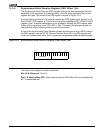
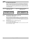
13.4.1 PIO Data Register 1 (PDATA1, Offset 7Ah)
Bits 7–0: PIO Data Bits (PDATA31–PDATA16)—This field determines the level driven on
each PIO pin or reflects the external level of the pin, depending upon whether the pin is
configured as an output or an input in the PIO Direction registers. The most significant bit
of the PDATA field indicates the level of PIO31, the next bit indicates the level of PIO30,
and so on.
The value of PDATA1 at reset is undefined.
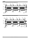
13.4.2 PIO Data Register 0 (PDATA0, Offset 74h)
Bits 15–0: PIO Data Bits (PDATA15–PDATA0)—This field is a continuation of the PDATA
field in the PIO Data 1 register.
The value of PDATA0 at reset is undefined.
13.5 OPEN-DRAIN OUTPUTS
The PIO Data registers permit the PIO signals to be operated as open-drain outputs. This
is accomplished by keeping the appropriate PDATA bits constant in the PIO Data register
and writing the data value into its associated bit position in the PIO Direction register, so
the output is either driving Low or is disabled, depending on the data.
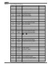
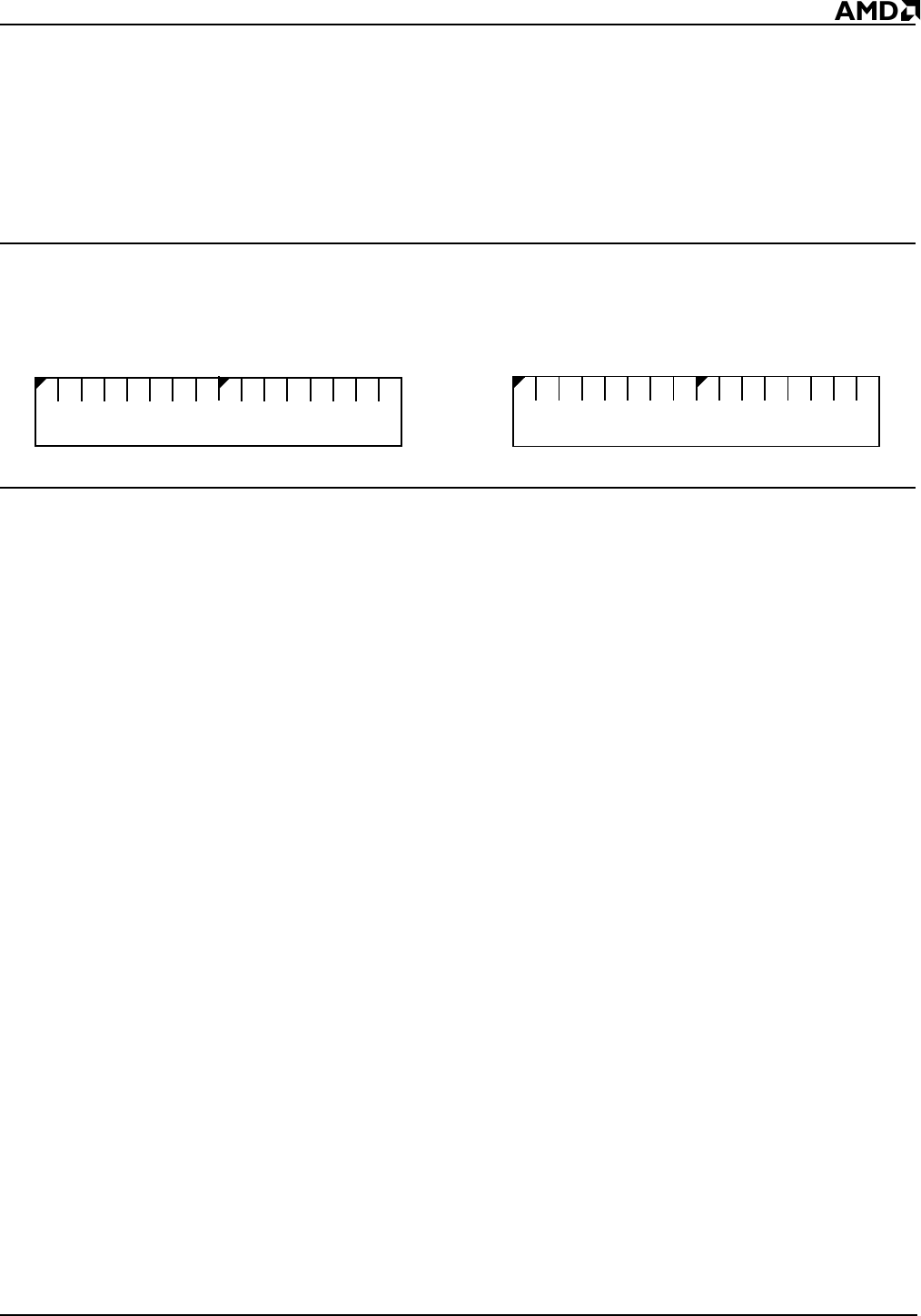
PDATA (15–0)
15 7 0
Figure 13-6 PIO Data 1 Register
(PDATA1, offset 7Ah)
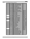
15 7 0
PDATA (31–16)
Figure 13-7 PIO Data 0 Register
(PDATA0, offset 74h)