


Chip Select Unit
5-13
microcontroller in which bit 6 was set with a meaningful value would not produce the address
expected on the Am186ER.
When the PCS
chip selects are mapped to I/O space, BA19–16 must be programmed to
0000b because the I/O address bus is only 16-bits wide.
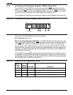
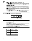
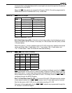
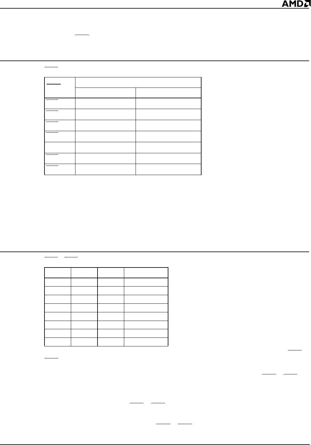
Table 5-5 PCS Address Ranges
Bits 6–4: Reserved—Set to 1.
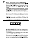
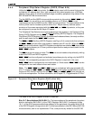
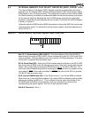
Bit 3: Wait-State Value (R3)—If this bit is set to 0, the number of wait states from zero to
three is encoded in the R1–R0 bits. In this case, R1–R0 encodes from zero (00b) to three
(11b) wait states.
When R3 is set to 1, the four possible values of R1–R0 encode four additional wait-state
values as follows: 00b = 5 wait states, 01b = 7 wait states, 10b = 9 wait states, and
11b = 15 wait states. Table 5-6 shows the wait-state encoding.
Table 5-6 PCS3–PCS0 Wait-State Encoding
Bit 2: Ready Mode (R2)—The R2 bit is used to configure the Ready mode for the PCS3–
PCS
0 chip selects. If R2 is set to 0, external ready is required. External ready is ignored
when R2 is set to 1. In each case, the processor also uses the value of the R3 and R1–R0
bits to determine the number of wait states to insert. The Ready mode for PCS
6–PCS5 is
configured through the MPCS Register.
Bits 1–0: Wait-State Value (R1–R0)—The value of R3 and R1–R0 determines the number
of wait states inserted into a PCS
3–PCS0 access. Up to 15 wait states can be inserted.
See the discussion of bit 3 (R3) for the wait-state encoding of R1–R0.
From zero to three wait states for the PCS
6–PCS5 outputs are programmed through the
R1–R0 bits in the MPCS Register.
PCS Line
Range
Low High
PCS
0 Base Address Base Address+255
PCS
1 Base Address+256 Base Address+511
PCS
2 Base Address+512 Base Address+767
PCS
3 Base Address+768 Base Address+1023
Reserved N/A N/A
PCS
5 Base Address+1280 Base Address+1535
PCS
6 Base Address+1536 Base Address+1791
R3 R1 R0 Wait States
000 0
001 1
010 2
011 3
100 5
101 7
110 9
111 15