


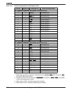
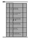
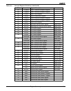
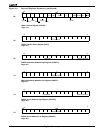
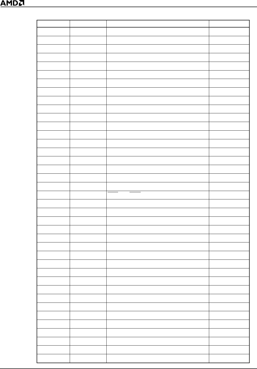
Register Summary
A-2
Table A-1 Internal Register Summary
Hex Offset Mnemonic Register Description Comment
FE RELREG Peripheral control block relocation register
F6 RESCON Reset configuration register
F4 PRL Processor release level register
F0 PDCON Power-save control register
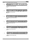
E4 EDRAM Enable RCU register
E2 CDRAM Clock prescaler register
E0 MDRAM Memory partition register
D8 D1TC DMA 1 transfer count register
D6 D1DSTH DMA 1 destination address high register
D4 D1DSTL DMA 1 destination address low register
D2 D1SRCH DMA 1 source address high register
D0 D1SRCL DMA 1 source address low register
CA D0CON DMA 0 control register
C8 D0TC DMA 0 transfer count register
C6 D0DSTH DMA 0 destination address high register
C4 D0DSTL DMA 0 destination address low register
C2 D0SRCH DMA 0 source address high register
C0 D0SRCL DMA 0 source address low register
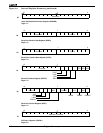
AC IMCS Internal memory chip select register
A8 MPCS PCS
and MCS auxiliary register
A6 MMCS Midrange memory chip select register
A4 PACS Peripheral chip select register
A2 LMCS Low memory chip select register
A0 UMCS Upper memory chip select register
88 SPBAUD Serial port baud rate divisor register
86 SPRD Serial port receive data register
84 SPTD Serial port transmit data register
82 SPSTS Serial port status register
80 SPCT Serial port control register
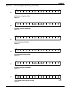
7A PDATA1 PIO data 1 register
78 PDIR1 PIO direction 1 register
76 PIOMODE1 PIO mode 1 register
74 PDATA0 PIO data 0 register
72 PDIR0 PIO direction 0 register
70 PIOMODE0 PIO mode 0 register
66 T2CON Timer 2 mode/control register
62 T2CMPA Timer 2 maxcount compare A register
60 T2CNT Timer 2 count register
5E T1CON Timer 1 mode/control register