


Chip Select Unit
5-2
Except for the UCS chip select, which is active on reset as discussed in section 5.5.1,
external memory chip selects are not activated until the associated registers have been
accessed by a write operation. The LCS
chip select is activated when the LMCS Register
is written, the MCS
chip selects are activated after both the MMCS and MPCS registers
have been written, and the PCS
chip selects are activated after both the PACS and MPCS
registers have been written.
5.2 CHIP SELECT TIMING
The timing for the UCS and LCS outputs has been modified from the 80C186 and 80C188
microcontrollers. These outputs now assert in conjunction with the demultiplexed address
bus (A19–A0) for normal memory timing. To make these outputs available earlier in the
bus cycle, the number of programmable memory size selections has been reduced.
The MCS
3–MCS0 and PCS chip selects assert with the AD bus.
5.3 READY AND WAIT-STATE PROGRAMMING
The Am186ER and Am188ER microcontrollers can be programmed to sense a ready signal
for each of the peripheral or memory chip select lines. The ready signal can be either the
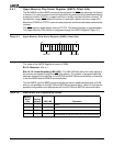
ARDY or SRDY signal. Each external chip select control register (UMCS, LMCS, MMCS,
PACS, and MPCS) contains a single-bit field, R2, that determines whether the external
ready signal is required or ignored. When R2 is set to 1, external ready is ignored. When
R2 is set to 0, external ready is required.
The number of wait states to be inserted for each access to a peripheral or memory region
is programmable. Zero wait states to 15 wait states can be inserted for the PCS
3–PCS0
peripheral chip selects. Zero wait states to three wait states can be inserted for all other
chip selects.
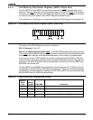
Each of the external chip select control registers other than the PACS Register (UMCS,
LMCS, MMCS, and MPCS) contains a two-bit field, R1–R0, whose value determines the
number of wait states from zero to three to be inserted. A value of 00b in this field specifies
no inserted wait states. A value of 11b specifies three inserted wait states.
The PCS
3–PCS0 peripheral chip selects can be programmed for up to 15 wait states. The
PACS Register uses bits R3 and R1–R0 for the additional wait states.
When external ready is required (R2 is set to 0), internally programmed wait states will
always complete before external ready can terminate or extend a bus cycle. For example,
if the internal wait states are set to insert two wait states (R1–R0 = 10b), the processor
samples the external ready pin during the first wait-state cycle. If external ready is asserted
at that time, the access completes after six cycles (four cycles plus two wait states). If
external ready is not asserted during the first wait state, the access is extended until ready
is asserted, which is followed by one more wait state followed by t
4
.
5.4 CHIP SELECT OVERLAP
Although programming the various chip selects on the Am186ER microcontroller so that
multiple chip select signals are asserted for the same physical address is not recommended,
it may be unavoidable in some systems. In such systems, the chip selects whose assertions
overlap must have the same configuration for ready (external ready required or not required)
and the number of wait states to be inserted into the cycle by the processor.
The peripheral control block (PCB) is accessed using internal signals. These internal signals
function as chip selects configured with zero wait states and no external ready. Therefore,
the PCB can be programmed to addresses that overlap external chip select signals if those
external chip selects are programmed to zero wait states with no external ready required.