


Synchronous Serial Interface
12-5
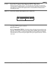
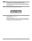
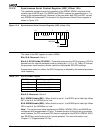
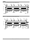
12.2.3 Synchronous Serial Transmit 1 Register (SSD1, Offset 14h)
Synchronous Serial Transmit 0 Register (SSD0, Offset 16h)
The Synchronous Serial Transmit 1 and 0 registers contain data to be transferred from the
processor to the peripheral on a write operation. Only the least-significant 8 bits of the
register are used. The format of SSD1 and SSD0 is shown in Figure 12-3.
Writes to SSD1 or SSD0 cause the PB bit in the SSS register to be set and a transmission
sequence to begin as shown in Figure 12-5 on page 12-8. A write to either SSD1 or SSD0
while the port is busy sets the RE/TE (Receive/Transmit Error) bit in the SSS register and
does not generate additional data transfers.
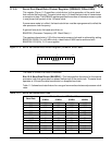
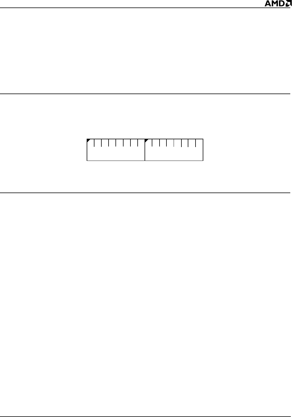
Figure 12-3 Synchronous Serial Transmit Register (SSD1, SSD0, offsets 14h and 16h)
The value of these registers at reset is undefined.
Bits 15–8: Reserved—Set to 0.
Bits 7–0: Send Data (SD)—Data to transmit over the SDATA pin. Bit 0 is transmitted first,
bit 7 is transmitted last.
15
70
Reserved
SD